This thread has been locked.

If you have a related question, please click the "Ask a related question" button in the top right corner. The newly created question will be automatically linked to this question.

DRV8705-Q1: Overcurrent fault behavior

Part Number: DRV8705-Q1
Other Parts Discussed in Thread: CSD18512Q5B, DRV8705S-Q1EVM,

Hello,

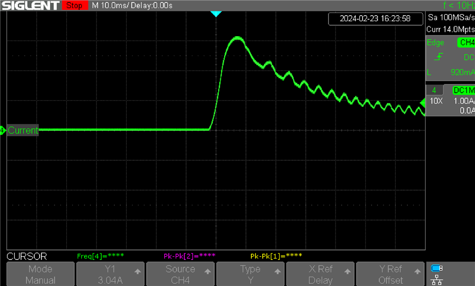
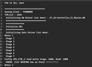
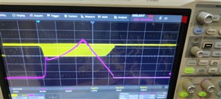
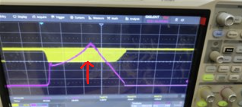
We are using the DRV8705SQRHBRQ1 motor driver in our application. Initially, we employed H-Bridge PWM Control, and the overcurrent fault was triggered correctly according to our current requirements. Subsequently, we switched to Half-Bridge Control for PWM mode, and after this modification, we did not observe an overcurrent fault. However, after adjusting the VDS overcurrent threshold, the overcurrent fault is now being triggered correctly

We want to know if changing the driver PWM modes affects the maximum current draw, or if there could be another reason for the change in the maximum current.

  • Hi Sonali,

    In half-bridge mode, only one motor phase is being controlled at a time, potentially leading to lower overall motor current compared to H-Bridge mode. This could indirectly make the VDS overcurrent protection less likely to trigger, since it responds to the voltage drop across the MOSFETs, which is related to current flow.

    Best,

    David

  • Hello Devid,

    Thank you for your response.

    Does operating the motor in half-bridge mode affect its torque and maximum speed? We don't want to get that affected.

    Thanks,

    Sonali

  • Hello Sonali,

    Could you please describe (a diagram will be helpful) the over current test you did and short circuit test path (if short circuit test was used for the over current test) with Full bridge FB and Hall Bridge HB configurations? In both cases, I assume the power supply did not have a current limit set. Was the DC motor load driven during the overcurrent test. What was the VDS threshold voltage values used for correct OC detection for FB and HB setup? Please also let us know the supply voltage value and the MOSFET part #. What were the Idrive settings used for the FETs? 

    In FB configuration you can have direction control of the BDC motor and in HB only one direction is possible. The maximum voltage and duty cycle with which the BDC motor can be driven would be about the same in both cases. With FB drive the motor will see supply voltage VM - 2x Rdson voltage drop across the FETs and with the HB drive VM - 1x Rdson voltage drop. The Rdson voltage drop will depend on the motor current. For example with a 5 mΩ FET and 10 A current the voltage drop across the FET would be 50 mV. So with VM = 12 V the FB motor voltage max would be 11.9 V and HB motor voltage max would be 11.95 V and both configurations support up to 100 % duty cycle operation. So maximum torque and speed would be almost the same in both use cases. Thank you.

    Regards, Murugavel        

  • Hello Murugavel,

    Set-up Explanation - The attached bridge circuit we are using to drive the DC motor. To produce an overcurrent event on the system, we detached the motor from the gearbox and connected it to the circuit. Subsequently, we applied power to the motor, causing it to rotate in one direction, all while securely holding the shaft in a vice grip. This resulted in the occurrence of the overcurrent event. This same process we are using for both FB and HB modes to trigger an overcurrent event.

    In both cases, I assume the power supply did not have a current limit set. - Yes

    Was the DC motor load driven during the overcurrent test - Yes

    What was the VDS threshold voltage values used for correct OC detection for FB and HB setup? for FB 0.06v, for HB 0.16v

    What were the Idrive settings used for the FETs? - 62mA for everything

    Please also let us know the supply voltage value and the MOSFET part # - CSD18512Q5B

    Let us know if you need more information.

    DRV8705S_MOTOR DRIVER SECTION.pdf

    Thanks,

    Sonali


  • Hello Sonali,

    Thanks for the details. So you are letting the motor stall which typically results with a very high current compared to the running current. Have you measured the motor stall current at this supply voltage? You can do this measurement by connecting the motor directly to the power supply. Holding it for longer periods might damage the motor winding. Were you using 100 % duty cycle in your tests? If not, what was the PWM frequency and duty cycle used for the tests?

    The output FETs used has very low Rdson, 1.3 mΩ, so voltage drop across them is very small. In FB 0.06V VDS tells me the peak current via the FET was 0.06/1.3E-3 = 46.5 A and in HB peak current with VDS 0.16V was 0.16/1.3E-3 = 123 A. In FB motor current passes through one HS and one LS FET vs. in HB motor current passes through only one FET. This would be the reason for increased current in HB. The increase observed seems excessive though. What is the DCR (DC resistance) specification of the DC motor?  

    I looked at the schematic and did not find any bulk capacitor on +24V Mot rail. For this motor you may need 100 to 200 uF. Are there capacitors on the power supply side close to the driver circuit? Bulk capacitor will help reduce the ripple on the +24V Mot when the motor is running and also reduce the load dump back to the power supply when the motor is stopped or speed is reduced.

    Regards, Murugavel

  • Hello Murugavel,

    Thank you for your response.

    We have measured the motor stall current by connecting the motor directly to the power supply, and it is up to 25A. We are attaching the stalling current waveform. The PWM frequency is set to 22kHz, and the duty cycle is 90%. Unfortunately, at the moment, we don't have information about the motor DCR specification as it is a custom design of our customer. Bulk capacitors of 470uF and 1uF are present on the power supply side, close to the driver circuit. A full schematic is attached for your reference.

    There is a small correction: previously, we were using PWM H-Bridge Control mode, and the VDS threshold voltage used for OC detection was 0.16V. Now, we are using PH/EN H-Bridge Control, and the VDS threshold voltage for OC detection is 0.06V.

    Are you suggesting that prolonged stalling might damage the motor? If so, could you please advise on the VDS threshold voltage we should set, considering our stall current and PH/EN H-Bridge Control, to avoid prolonged stalling?

      DRV8705S_Schematic.pdf

    Thanks,

    Sonali

  • Hi Sonali,

    Thank you for the information. Let me review and get back to you.

    Regards, Murugavel

  • Hello Murugavel,

    Is there any update on this?

    Thanks,

    Sonali

  • Hello Sonali,

    Monday was a US holiday. We were unable to get back to you yesterday. I'll send you my reply today. Thanks.

    Regards, Murugavel

  • Hello Sonali,

    Technically PH/EN mode and PWM mode should behave the same as long as the control logic and freewheel option selected are identical. Do you use high side or low side active freewheeling? Are they same in both PH/EN and PWM modes?

    If I understood correctly independent half-bridge was not used. Only PH/EN and PWM modes FB were used. Is my understanding correct?

    Regarding over current limit setting - this will depend on the purpose of the detection. If it will be used for stuck motor (stall) detection we need to make sure if also satisfies start up inrush current. Otherwise the bridge may be disabled at startup is latched fault mode is selected or the drive may be interrupted is cycle by cycle OCP mode is selected. 

    When the motor is permanently stalled with a vise the inrush current will be much higher and also will be this high value for a longer period of time if the OCP does not trip. Only in those conditions the motor will overheat and damage. 

    For normal OCP setting for BDC motors the method would be to characterize the motor startup inrush current and set the limit higher than that value with sufficient margin to cover motor to motor variation. 

    Another source of high current is the active freewheeling recirculation current and current when the motor is reversed or stopped without a deceleration stop motion profile. The stored mechanical potential energy will flow through the FETs and could get very high depending on the potential energy (motor speed) and the motor itself.

    I reviewed the schematic and I did not notice anything unusual. 

    Regards, Murugavel 

  • Hello Murugavel,

    Thank you for your response.

    Here is a little more information. Earlier, we set 20A current through internal ADC in firmware. We get the expected overcurrent fault at 20A current. Now, we are not getting overcurrent fault at 20A current. Therefore, we lower the current limit to 15A and get the overcurrent fault. 

    What could be the reason for changing the maximum current draw? Thus, the PWM mode we are using i.e. PH/EN and PWM modes affects the maximum current draw or there could be any other reason?

    Thanks,

    Sonali

  • Hello Sonali,

    Thanks for getting back on this. You asked "the PWM mode we are using i.e. PH/EN and PWM modes affects the maximum current draw or there could be any other reason?" as long as the active freewheeling is done the same way it won't be different. In PWM mode both inputs must be 100% duty (HIGH) when motor is not running and for 90% duty output one of them must be 10% duty (10 % high and 90 % low). This will maintain same polarity as PH/EN. If this is adhered to, both PH/EN and PWM modes would behave the same way. I verified this with a DRV8705S-Q1EVM and a DC motor.

    Regards, Murugavel 

  • Hello Murugavel,

    The freewheeling is the same for both modes i.e. low-side freewheeling. 

    If not PWM mode, what could be another reason for changing the max current?

    Thanks,

    Sonali

  • Hello Sonali,

    I did extensive testing with a battery source with no current limiting with a BDC motor and the EVM. I found the behavior of the PH/EN and PWM modes were identical. Freewheeling was set to low-side for both tests. The OCP threshold, VDS = 0.06 V made the startup current (almost equal to the BDC motor stall current) to trip the OCP limit occasionally. I could make the OCP trip more consistent if I reduced the VDS_DG to 1 us. Increasing the VDS = 0.08 I did not see OCP tripping in both PH/EN and PWM modes during startup. It was consistent. I am unable to reproduce the level of difference of VDS threshold you were experiencing between the two modes. The measured average DC voltage on the OUT pin at 90 % duty cycle was identical in both the cases, PH/EN and PWM. Were you observing the difference while running the motor in the same direction?

    The startup inrush current was higher in one direction of the motor vs. the other - this could be because of differences in friction of the rotor one direction vs. the other. However running the motor in the same direction in both PH/EN and PWM modes had the same current profile at startup and same OCP behavior in my setup with an EVM. 

    You said "Earlier, we set 20A current through internal ADC in firmware. We get the expected overcurrent fault at 20A current. Now, we are not getting overcurrent fault at 20A current. Therefore, we lower the current limit to 15A and get the overcurrent fault.". Could you please elaborate this statement? Are you using the CSA output analog voltage information, convert it to digital using the MCU ADC and determine whether the current exceeded the set threshold or not, is this correct? If you were using this approach you may not get consistent results unless you successfully captured the peak current at the exact instant. How was the ADC triggered to capture the peak value consistently? 

    Regards, Murugavel 

  • Hello Murugavel,

    Are you using the CSA output analog voltage information, convert it to digital using the MCU ADC, and determine whether the current exceeded the set threshold or not, is this correct?  -- Yes, correct

    How was the ADC triggered to capture the peak value consistently? -- We consistently capture the peak value by implementing constant sampling at a 10ms period. 

    One more question: Does the CSA_GAIN change the maximum current draw? If yes, how does the gain affect the maximum current?

    Also, we would like to know the CSA output in our schematic design in case of gain = 10V/V and gain = 20V/V.       .... CSA_DIV = 0b = AREF / 2

    Let me know if you need more information.

    Thanks,

    Sonali

  • Hi Sonali,

    Thanks for the update and additional details. Please see below scope captures of the inrush current in PH/EN mode and PWM mode for the same motor, 24V motor supply and with 90 % duty cycle 20 kHz PWM.

    PH/EN mode:

    PWM mode:

    You can see the inrush current peak is about 30 A and pretty similar in profile in both modes. You can also notice the peak lasts only a few ms. With 10ms sample rate it is impossible to capture the true peak value consistently. Ideally you should sample once every 0.5ms to capture the peak consistently. 

    CSA gain does not change the maximum current output. CSA is only for sensing and outputting analog voltage on SO. 

    In your circuit the current sense resistor is 0.004Ω. So for 1A current flow the voltage on the SP will be 0.004V. AREF = 3.3V, AREF/2 =  1.65V. For 0A current the SO will be 1.65V. For 1A current flow, with gain 10V/V SO will be 1.65 + (0.004*10)= 1.69V, with gain 20V/V SO will be 1.65 + (0.004*20) = 1.73V.  So for 25A current flow SP will be 0.1V, with gain 10V/V SO will be 1.65 + (0.1*10)= 2.65V, with gain 20V/V SO will be 1.65 + (0.1*20) = 3.65V which will be > 3.3V. So the SO will saturate at 3.3V. Gain 20V/V cannot be used to capture the startup peak. 

    Have you looked at the SO waveforms for both modes and verified the startup current profile is as expected. 

    For OCP detection and protection we suggest to use on chip VDS monitors because it will have the fastest response, just a few μs considering the deglitch time.

    Regards, Murugavel

  • Hello Murigavel,

    Thank you for your quick response.

    Have you looked at the SO waveforms for both modes and verified the startup current profile is as expected. -- No, but this will be our next step.

    In the end, you can find our register mapping in the firmware, and our board is currently operating correctly with this configuration.

    However, upon changing the CSA_GAIN to 10V/V while keeping the other mappings unchanged, we encountered an error during driver initialization. The error message is as follows: 'Config VDS_CTRL_2 read-write stage: 4A00, Read: C000'. Please refer to the attached image for details.

    Could you kindly explain why changing only the gain is resulting in this error? Additionally, we would like to understand which parameters are affected by the gain in the mapping. 

    Error image:

    Register Mapping: 

    /* DRV8705 driver SW module constructor, linking also system timer/counter */
    drv8705Module[0].configData.clr_flt = CLEAR_FAULTS_N_RESET;
    drv8705Module[0].configData.lock = UNLOCK_CONTROL_REGISTERS;
    drv8705Module[0].configData.in2_ph_mode = SIGNAL_SOURCED_FROM_IN2_PH_PIN;
    drv8705Module[0].configData.in1_en_mode = SIGNAL_SOURCED_FROM_IN1_EN_PIN;
    drv8705Module[0].configData.ssc_dis = DEVICE_SPREADSPECTRUM_CLOCKING_ENABLE;
    drv8705Module[0].configData.en_drv = DRIVER_OUTPUTS_ENABLE_N_CONTROL_BY_DIGITAL_INPUTS;
    drv8705Module[0].configData.s_hiz2 = OUTPUTS_FOLLOW_IN2_PH_SIGNAL;
    drv8705Module[0].configData.s_hiz1 = OUTPUTS_FOLLOW_IN1_EN_SIGNAL;
    drv8705Module[0].configData.s_in2_ph = CONTROL_BIT_FOR_IN2_PH_INPUT_SIGNAL_ENABLED_THROUGH_IN2_PH_MODE_BIT;
    drv8705Module[0].configData.s_in1_en = CONTROL_BIT_FOR_IN1_EN_INPUT_SIGNAL_ENABLED_THROUGH_IN1_EN_MODE_BIT;
    drv8705Module[0].configData.brg_fw = LOW_SIDE_FREE_WHEELING;
    drv8705Module[0].configData.brg_mode = PH_EN_HALF_BRIDGE_INPUT_CONTROL;
    drv8705Module[0].configData.vgs_hs_dis = ENABLED;
    drv8705Module[0].configData.IDRVN_HS = High_side_peak_sink_pull_down_current_62mA;
    drv8705Module[0].configData.IDRVP_HS = High_side_peak_source_pull_up_current_62mA;
    drv8705Module[0].configData.IDRVN_LS = low_side_peak_sink_pull_down_current_62mA;
    drv8705Module[0].configData.IDRVP_LS = low_side_peak_source_pull_up_current_62mA;
    drv8705Module[0].configData.VGS_IND = Disabled;
    drv8705Module[0].configData.VGS_TDEAD = Insertable_digital_dead_time_500ns;
    drv8705Module[0].configData.VGS_TDRV = VGS_drive_time_and_VDS_monitor_blanking_time_4us;
    drv8705Module[0].configData.VGS_MODE = VGS_gate_fault_monitor_mode_Latched_fault;
    drv8705Module[0].configData.VDS_IND = VDS_independent_shutdown_mode_Disabled;
    drv8705Module[0].configData.VDS_IDRVN = DRVN_gate_pulldown_current_after_VDS_OCP_fault_Programmed_IDRVN;
    drv8705Module[0].configData.VDS_DG = VDS_overcurrent_monitor_deglitch_time_8us;
    drv8705Module[0].configData.VDS_MODE = VDS_overcurrent_monitor_mode_Latched_fault;
    drv8705Module[0].configData.VDS_LS_LVL = Low_side_VDS_overcurrent_monitor_threshold_0_16v;
    drv8705Module[0].configData.VDS_HS_LVL = High_side_VDS_overcurrent_monitor_threshold_0_16v;
    drv8705Module[0].configData.PD_SH2 = Half_bridge_2_pull_down_diagnostic_current_source_Disabled;
    drv8705Module[0].configData.PU_SH2 = Half_bridge_2_pull_up_diagnostic_current_source_Disabled;
    drv8705Module[0].configData.PD_SH1 = Half_bridge_1_pull_down_diagnostic_current_source_Disabled;
    drv8705Module[0].configData.PU_SH1 = Half_bridge_1_pull_up_diagnostic_current_source_Disabled;
    drv8705Module[0].configData.OLSC_EN = Offline_open_load_and_short_circuit_diagnostic_Disabled;
    drv8705Module[0].configData.VCP_UV_LVL = VCP_charge_pump_undervoltage_monitor_threshold_2_5v;
    drv8705Module[0].configData.VCP_UV_MODE = VCP_charge_pump_undervoltage_monitor_mode_Latched_fault;
    drv8705Module[0].configData.PVDD_OV_LVL = PVDD_supply_overvoltage_monitor_threshold_28_5v;
    drv8705Module[0].configData.PVDD_OV_DG = PVDD_supply_overvoltage_monitor_deglitch_time_8us;
    drv8705Module[0].configData.PVDD_OV_MODE = PVDD_supply_overvoltage_monitor_mode_Latched_fault;
    drv8705Module[0].configData.PVDD_UV_MODE = PVDD_supply_undervoltage_monitor_mode_Latched_fault;
    drv8705Module[0].configData.CSA_GAIN = Current_shunt_amplifier_gain_setting_20_VV;
    drv8705Module[0].configData.CSA_DIV = Current_shunt_amplifier_reference_voltage_divider_AREF_2;
    drv8705Module[0].configData.CSA_BLK = Current_shunt_amplifier_blanking_time_of_tDRV_0_Disabled;
    drv8705Module[0].configData.CSA_BLK_SEL = Current_shunt_amplifier_blanking_trigger_source_Half_bridge_1;
    drv8705Module[0].configData.CSA_SH_EN = Current_shunt_amplifier_sample_and_hold_Disabled;

    driver3phSWI[0] = new_drv8705(&drv8705Module[0], sysHwDevDriver.drv8705HWI[0],
    sysHwDevDriver.systemCntrHWI);

    Thanks,

    Sonali

  • Hello Sonali,

    The CSA in the DRV8705-Q1 is a separate entity that provides analog output on SO. Changing the CSA_CTRL Register does not interact with the device operation or any other registers unless the external MCU takes some action based on SO value. In the EVM changing through all the gain options does not interfere with the device operation. It changes only the SO value and the ADC reading based on SO value - expected behavior. 

    Writing to CSA_CTRL does not change anything in the VDS_CTRL_2 register. Status read value 0xC000 means no SPI error and a POR condition was detected. POR means the DVDD voltage dipped below VDVDD_POR DVDD falling threshold and the device was reset. Can you check what was happening to DVDD during this time? A POR condition would reset all the registers of the device to its default values. POR must not happen during normal operation.

    Regards, Murugavel  

  • Hello Murugavel,

    We haven't seen voltage dipped on DVDD voltage. See attached DVDD waveforms. 

    As you mentioned, changing the gain does not affect other device operations. I have consulted the firmware team to confirm if the MCU takes any action based on the SO value. They clarified that the ADC is solely gathering current and does not initiate any actions. As our motor's maximum current is 25A, we should set the gain to 10V/V, but we are getting an error on this setting. 

    Tomorrow, we plan to test the SO signal. Using hardware calculation, we will assess the maximum current draw of the motor through the SO value. We will then compare the calculated current with the ADC current to check for a match. Please let us know if there is an alternative method for testing.

    Regarding the SO equation, you provided AREF/2 + [(SP-SN) * GAIN]. It is correct?

    But you can see our schematic, we have connected S1_P to SN (pin 19) and S1_N to SP (pin 18) of the driver. This will change the SO equation, AREF/2 - [(SN-SP) * GAIN]. Let me know which equation is correct for our schematic. We need this for tomorrow's test.

    Note: Our primary concern is that the maximum current drawn has changed. Previously, the motor drew up to 25A, but now it seems to be limited to 15A.

    Thanks,

    Sonali


  • Hello Sonali,

    The below portion of the schematic shows S1_P and S1_N correctly. I assumed it was connected correctly to the device SP and SN respectively. Only after you mentioned in your message I noticed you had the netlist names swapped at U4A. This would not work correctly. 

    You can also see SP and SN described clearly in pin description, page-5 of the datasheet. SP and SN must not be interchanged. It is not designed to work with interchanged connection. Based on the present connection of your schematic, SO does not output the sense voltage as described. This must be fixed in your board. See below functional block diagram from the datasheet as well.

    The sense resistor in your schematic R28 is 0.004Ω. So SO = (AREF/2) + (ILOW-SIDE * 0.004Ω) * GAIN. The load current flowing through one of the LS FETs to GND at any given direction of operation of the bridge will be presented to SP and SN. SN must always be GND. SP is connected to the positive end of the shunt resistor R28. Voltage (ILOW-SIDE * 0.004Ω) = SP-SN voltages, SN = 0V. 

    Changing GAIN values in CSA_CTRL register should neither interfere with any other register nor cause any issues because CSA is used for measuring and reporting analog voltage equivalent to the shunt resistor current. You may want to check if the CSA register address was properly defined in the firmware and not point to some other address.

    While you can use SO to get current reading, because of blanking etc. it may not be a true representation for calculation purpose. It would be better to measure the current waveform between GND end and top end of the sense resistor R28, if you do not have a non-contact current probe. The voltage output measured would be I * 0.004Ω. 

    Regards, Murugavel

  • Hello Murugavel,

    Below are our testing results, along with the attached images:

    • Normal operation motor current: 1.22A ... Voltage drop across the sense resistor: 4.9mV
    • Stall motor current: 22.5A ... Voltage drop across the sense resistor: 99mV
    • SO output:
      • Motor OFF: 1.43V
      • Motor ON: 1.34V

    I believe the current we measured at the sense resistor is as expected. The issue lies with the SO output, which should be 1.65V, correct? Tomorrow, I will check our VREF voltage.

    Due to swapped SN and SP connections, the SO output is dropping from 1.43V to 1.34V. We can measure the current through ADC with this connection. At this last moment, we don't want to change the design.

    Please let me know if these connections can still work. If yes, could you please provide the SO formula?

    We have measured the motor current below using current probes compatible with oscilloscopes

    1) Motor current and SO voltage waveforms on normal operation. 

    Pink: motor current, Yellow:  SO voltage

    2) Motor current and SO voltage waveforms on stall conditions.

    Pink: motor current, Yellow:  SO voltage

    Thanks,

    Sonali

  • Hello Sonali,

    Thanks for sharing measurement data. You said "The issue lies with the SO output, which should be 1.65V, correct? Tomorrow, I will check our VREF voltage.". Yes correct and 1.65V is based on AREF = 3.3V per your schematic. So AREF/2 = 1.65V. 

    "Due to swapped SN and SP connections, the SO output is dropping from 1.43V to 1.34V. We can measure the current through ADC with this connection. At this last moment, we don't want to change the design. Please let me know if these connections can still work. If yes, could you please provide the SO formula?". We'll have to check with the inner design and confirm if this will not affect the functionality of CSA as well as we can confirm the formula. We can try to get this information by mid next week.

    Based on this scope capture the SO is saturated at GND potential 0V. The CSA GAIN must be reduced to ensure the CSA output is not saturating (clipped at 0). The peak value and the waveform should resemble the pink trace but would look inverted because of your SN and SP connections.

    Regards, Murugavel

  • Hello Sonali,

    Here's an update regarding the DRV8705-Q1 CSA. Swapping of SN and SP should not cause any electrical issues. It should work fine. The output would be [1.65 - (Ishunt*Rshunt*GAIN)] V, with AREF = 3.3V and AREF/2 selected for bias, and with current flow direction via shunt resistor from SN node (sense voltage +) to SP node (GND sense 0V ground reference).

    Regards, Murugavel

  • Hello Murugavel, 

    Thank you for the confirmation. 

    The VREF 

    You may want to check if the CSA register address was properly defined in the firmware and not point to some other address. -- I have confirmed this with the firmware team. The address is defined properly.

    For 10V/V gain we are getting the error Config VDS_CTRL_2 read-write stage: 4A00, Read: C000. But in our case, changing the gain is affecting other parameters. Also, there is no dipped in DVDD. What could be another reason for this? What should we test next?

    Thanks,

    Sonali


  • Hello Sonali,

    What was the VREF voltage? Why was SO 1.43V while motor off instead of 1.65V?

    Config VDS_CTRL_2 4A00 implies you were reading register address 0xA, VDS_CTRL_2. The read value you indicated was 0xC000. This tells me there was no fault (0xC0) and the VDS thresholds were set to 0.06V which would be the lowest setting for the on-chip VDS monitors for over current. 

    What is the setting for VDS_MODE bits in VDS_CTRL_1 register. If you were not using on-chip VDS monitor it should be 11b. If it was other values then VDS_CTRL_2 values must be set appropriately to avoid an unnecessary OCP detect.


    Like I said there is no issues in changing the CSA GAIN in the EVM that affects other registers. The DRV8705S-Q1 is widely used by several customers. Were you able to repeat this issue with more than one hardware? Do you happen to have an EVM to double check? Please take a look at your firmware in detail as well use an SPI sniffer tool such as Saleae or an oscilloscope with SPI decoder to see / capture while writing to CSA_CTRL if there were other unintended writes to registers performed.

    Regards, Murugavel

  • Hello Murugavel,

    What was the VREF voltage? Why was SO 1.43V while motor off instead of 1.65V? -- We have checked the VREF, and it's getting dropped to 2.86V. We have used a 15mA shunt reference to generate a 3V3 supply and the current requirement on 3V3 is up to 40mA. That is why VREF is getting dropped to 2.86V. We have connected the external 3.3V supply to VREF. Now we get SO 1.65V.

    We encountered a firmware issue related to reading register values, but we have successfully resolved the error. Consequently, we can now change CSA_GAIN to 10V/V, and our overcurrent issue has been resolved. Now, we are getting overcurrent fault at 20A and 25A as well. 

    For ADC conversion, we use the below formula.

    return (float)(20.625F - (adc_in * 0.010071))                ....gain of 20V/V and Rsense of 0.004 ohms

    This formula accounts for a maximum current of 20.625A.

    Now, with the gain changed to 10V/V, the updated ADC conversion formula is as follows:

    return (float)(41.25F - (adc_in * 0.020141601))

    Could you please confirm whether this new formula is accurate? Additionally, what does the parameter 0.010071 represent in the original formula?

    Thanks,

    Sonali

  • Hello Sonali,

    Thank you for the update. I'm glad you were able to identify the issues and resolve all of them including the overcurrent issue.

    For your system the SO voltage would be [1.65 - (Ishunt*Rshunt*GAIN)] V. For 1A, SO = 1.65 - (1 * 0.004 * 10) = 1.61V. The actual voltage difference for 1A would be 1.65-1.61 = 0.04V or in other words current in amps = [(1.65 - SO) / 0.04] A. 

    I believe the ADC in the MCU is 12-bits with VREF = 3.3V meaning 0V = 0 and 3.3V = 4095. So to get the SO voltage reading from the counts, SO = (counts*3.3)/4095 V.

    Current =  [1.65 - ((counts*3.3)/4095)] / 0.04 A which is, = (41.25 - counts*0.02014652) A. These calculations must be performed in floating point to avoid loss of precision. For achieving accuracy it is important 3.3V VREF is precise enough.

    Please mark this e2e post as resolved and close it at your end. Thanks.

    Regards, Murugavel


  • Hello Murugavel,

    Thank you for your support.

    Why are you using 4095, while we are using 4096 for calculation?

    Thanks,

    Sonali

  • Hello Sonali,

    You are welcome. This is from the 12-bit ADC in the microcontroller. The maximum count for 12-bits will be (2^12 - 1) = 4095, range will be 0 to 4095 counts.

    Regards, Murugavel