- Ask a related questionWhat is a related question?A related question is a question created from another question. When the related question is created, it will be automatically linked to the original question.
This thread has been locked.
If you have a related question, please click the "Ask a related question" button in the top right corner. The newly created question will be automatically linked to this question.
Hi Team,
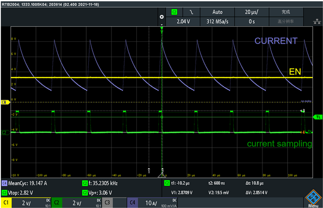
The customer tried to short-circuit the two poles of the motor. At this time, the peak current could reach 40A (the designed current limit value is 8A), and the frequency of the peak current was 35KHZ. At this time, the nfault pin was still at high level, and no error was reported to shut down the output.
After replacing different power supplies and batteries, the results are the same.
1. Why is the frequency of peak current 35KHZ?
2. Why is the nfault pin still high after exceeding the hardware current limit?
Current waveform
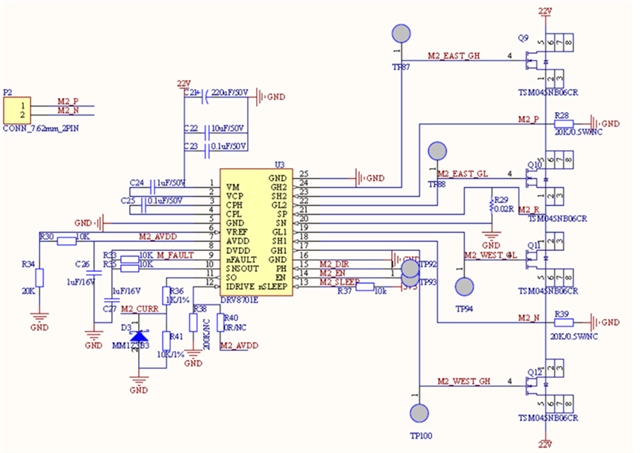
Schematic diagram
May I ask why this phenomenon occurs?
Regards,
Annie
Hi Annie,
You said "(the designed current limit value is 8A)". By calculation with R30 and R34 it works out to 7.875A, so ~8A.
For ICHOP current regulation there is a blanking time of 2us (see datasheet). Current regulation comparator detection is valid only after this time expires. Current regulation is done by fixed TOFF chopping. TOFF is specified 25us typical. With this customer test case, because of the short circuit and the low Rdson of the FETs the current is reaching a much higher peak during the 2us blanking time. Based on the scope capture you shared the current peak looks like ~32A. The ICHOP comparator has detected that current has exceeded set value immediately after 2us blanking time and does a TOFF chopping of 25us.This pattern is repeated continuously resulting in a (2 + 25) 27us time period which works out to ~37kHz.
With proper motor load the current will rise much slower so after tBLANK the current would still be < target ~ 8A. So there will be tDRIVE until the load current reaches ICHOP level and then have a TOFF. This would be expected behavior with a BDC motor load.
The reason there was no nFAULT during the short circuit test was the OCP threshold was never reached. For OCP to be detected either VDS should reach 1V or VSP (across sense resistor) should reach 1V. Rsense = 0.02Ω, so for 1V VSP the current peak has to be 1/0.02 = 50A. This was never reached. If the customer changed Rsense = 50mΩ then VSP will be 1V at 20A, so >20A will detect an OCP after tOCP. It is possible by the time tOCP expires the current may be much higher than 20A when OCP shuts down the output. For 50mΩ customer can modify VREF to achieve 8A for ICHOP.
The FETs used were TSM045NB06CR which have Rdson = 5mΩ. For VDS = 1V the current through the FETs has to be 1/0.005 = 200A! So VDS threshold will never be reached for 40A short circuit current.
Note: Not sure if IDRIVE pin was connected to AVDD with a 0Ω. If so OCP monitor on the high-side FETs is disabled.

Regards, Murugavel
Hi Murugavel,
He changed RSENSE to 50mΩ, VSP=1V when current = 20A.
ICHOP=(VREF-VOFF)/AV*RSENSE
If the current is limited to 8A, the corresponding VREF will reach 8V, and the value of VREF in the manual is 0.3V-AVDD, and the maximum voltage of AVDD is 4.8V, so the current limit of 8A cannot be realized.
Could you please indicate your suggestion this question?
Regards,
Annie
Hi Annie,
I gave the explanation for the behavior and ways to have OCP at 20A just because customer was using a very low Rdson FETs.
Because of fixed gain for AV, the DRV8701 cannot do both 8A ICHOP and 20A current OCP. Customer has to identify a tradeoff. Alternative option would be to pick Rdson of the FET to have VDS = 0.8A at OCP current of interest. For example for 30A VDS_OCP trip 0.8/30 = ~26mΩ.
Other options would be to consider DRV8705-Q1 or DRV8706-Q1 or a fully integrated MOSFETs BDC drivers DRV8262 would be another option.
Regards, Murugavel
Hi Murugavel,
According to the manual, the time to detect OCP should be greater than 4.5us.
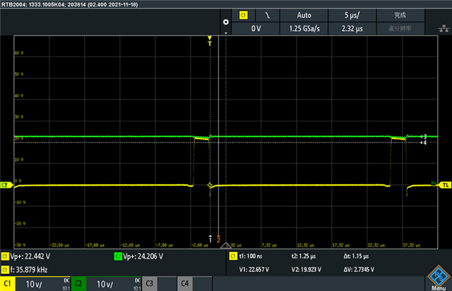
Hi Annie,
"The customer tested the waveform of D and S of Q12 against GND in the schematic diagram when the FET is short-circuited.". Green is 22V DRAIN of Q12 according to the schematic. Based on the scope capture, it looks like when Q12 was conducting for ~2.5us, the SOURCE of Q12 was close to 22V or VDS was a small voltage level not enough to trigger a VDS_OCP. When Q12 is not conducting for about 25us the VDS was 22V.
VDS_OCP monitor is active only while the FET is conducting, not while it is not conducting. For the record, a VDS level = 1V for a 5mΩ FET in hard switch on conduction, suggests a current flow of 1/0.005 = 200A.
You mentioned, "when the FET is short-circuited" Which FET was short circuited? Q11?
Regards, Murugavel
Hi Murugavel,
The customer did another test and found that the FET conduction time corresponds to the high level time of current sampling. This time seems to be blanking time, but is actually about 2.5us. That is to say, when the two poles of the motor are short-circuited with wires, the actual switching frequency of the FET is consistent with the current sampling, which is 2.5us on time, and then 25us off time. In this case, if VDS is used to monitor overcurrent, even if a FET with a larger Rdson is used, the time does not seem to be able to meet the detection requirements of OCP (4.5us). Does this mean that using VDS to monitor overcurrent is not as effective as VSP?
Regards,
Annie
Hi Annie,
Assuming the customer tested with the updated Rsense = 50mΩ.
Based on R30 = 10k and R34 = 20k, VREF = (AVDD/30k)*10k = 4.8/3 = 1.6V. ICHOP=(VREF-VOFF)/AV*RSENSE = (1.6 - 0.050)/(20*0.050) = 1.55A. I think tON for 1.55A was PWM blanking time of 2us + 0.5us = 2,5us during which FET Q12 was ON and then tOFF = 25us Q12 was OFF. This current regulation PWM pattern repeated as per the scope capture.

The VSP_OCP threshold of 20A (with 50mΩ Rsense) was never reached. So no OCP reported. Because the current regulation will always kick in first VSP_OCP will never be reached unless the current regulation is disabled in this device. If the current regulation feature is not needed, it can be disabled by tying VREF directly to AVDD and tying SP and SN to GND.
Let's assume the VREF is connected to AVDD directly, 4.8V. To achieve 8A Ichop Rsense needed would be 4.75/(2*8) = 29.6875 mΩ = approx. 30mΩ. With a 30mΩ and 4.8V VREF close to 8A Ichop can be achieved. Using this resistor the VSP_OCP threshold would be 1/0.03 = 33.33A. Note, VSP_OCP can be reached only if the current regulation is disabled.
For the 5mΩ FET Rdson, VDS_OCP = 1/0.005 = 200A, this can never me reached. VSP_OCP threshold would be reached before the VDS_OCP in this situation, granted the Ichop current regulation is disabled. If Ichop current regulation is enabled then VSP_OCP will never happen. This is not an issue, no concerns here. This also means nFAULT will not report the short circuit condition. If this reporting is needed we have to identify another device in our portfolio that will be suitable for this application.
In some applications, Rsense is not used and SP and SN is tied to GND to disable current regulation. In this case VDS_OCP will be the only protection from over current. However with very low Rdson FETs this current could be significantly higher if the power supply can provide it. With this device it would be better to use higher Rdson FETs to achieve a reasonable level of OCP protection current.
This is how the DRV8701 is expected to work. I hope this explanation covers all the information required to design with this device. Thanks.
Regards, Murugavel
Hi Murugavel,
Customer wants to know how the SO pin of DRV8701 works?
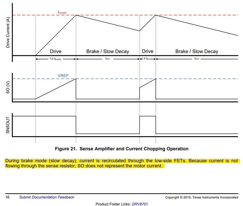
It can be seen from the screenshot of the oscilloscope that when the current is chopped, the voltage collected by the voltage dividing sampling point of SO directly becomes 0. This causes the MCU to think that the current is also 0 at this time, but it is not actually the case.
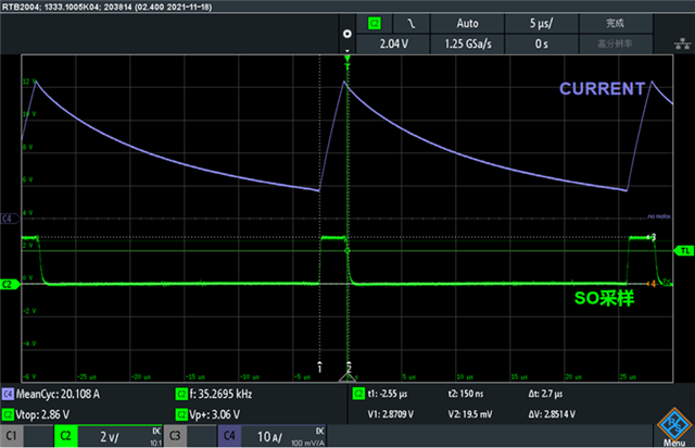
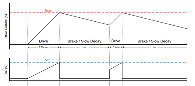
According to the manual, SO should also have a certain voltage during tooff time, not 0. Why can't the voltage of SO be collected during tooff time?
Regards,
Annie
Hi Annie,
This is expected behavior. Customer must ignore the SO output during tOFF. While the inputs of the amp is 0, SO will have some offset according to the datasheet specifications. When SP and SN are connected to the sense resistor the offset could change.
Regards, Murugavel