This thread has been locked.

If you have a related question, please click the "Ask a related question" button in the top right corner. The newly created question will be automatically linked to this question.

DRV8462: DRV8462

Part Number: DRV8462
Other Parts Discussed in Thread: DRV8426

Hi,

  • I am having trouble with SPI communication with the DRV8426 - MODE and nSLEEP is HIGH.
  • SPI read command for FAULT register returns 1 for FAULT & SPI_ERROR - however the data packet seems correct as using SPI mode 1 and nSCS is low when there is a data packet?
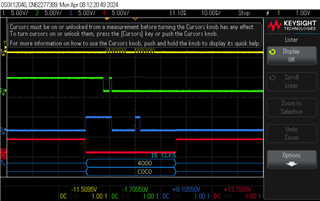
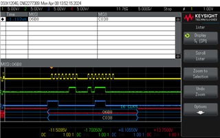
  • I have tried clearing the fault via CLR_FLT bit or an nSLEEP reset pulse - unsure if the write works as wrote 0x06B8 and returns 0xC038 is this correct?
  • Read Command 0x0400 return 0xC0C0 should be 0xC000 - correct?

  ]

Thanks in advance,

Phillip Bothma

  • Hey Phillip, give us another day to look into this, apologies.

    Make sure you're following the SPI format requirements.  This typically corresponds to the standard of "SPI Mode 1", where CPOL=0 and CPHA=1, output edge rising and data capture falling. 

    Best,

    Jacob

  • Perhaps this example code from our EVM will also help:

    // Direct writing of a register
    void DRV8462::writeRegister(uint8_t reg, uint8_t value)
    {
      write8(reg, value);
    }
    
    // These defines are in the .h file
    // SPI Protocol
    #define SPI_ADDRESS_MASK   0x3F00        // Mask for SPI register address bits
    #define SPI_ADDRESS_POS    8             // Position for SPI register address bits
    #define SPI_DATA_MASK      0x00FF        // Mask for SPI register data bits
    #define SPI_DATA_POS       0             // Position for SPI register data bits
    #define SPI_RW_BIT_MASK    0x4000        // Mask for SPI register read write indication bit
    
    void DRV8462::write8(uint8_t reg, uint8_t value) {
    
      // This SPI function is used to write the set device configurations and operating
      // parameters of the device.
      // Register format |R/W|A5|A4|A3|A2|A1|A0|*|D7|D6|D5|D4|D3|D2|D1|D0|
      // Ax is address bit, Dx is data bits and R/W is read write bit.
      // For write R/W bit should 0.
    
      volatile uint16_t reg_value = 0; // Variable for the combined register and data info
      reg_value |= ((reg << SPI_ADDRESS_POS) & SPI_ADDRESS_MASK);         // Adding register address value
      reg_value |= ((value << SPI_DATA_POS) & SPI_DATA_MASK);             // Adding data value
    
      digitalWrite(_cs, LOW);
    
      SPIxfer((uint8_t)((reg_value>>8) & 0xFF));
      SPIxfer((uint8_t)(reg_value & 0xFF));
    
      digitalWrite(_cs, HIGH);
    }
    
    uint8_t DRV8462::SPIxfer(uint8_t x) {
      if (_clk == -1) {
        return _spi->transfer(x);
      } else {
        // Serial.println("Software SPI");
        uint8_t reply = 0;
        for (int i = 7; i >= 0; i--) {
          reply <<= 1;
          digitalWrite(_clk, HIGH);
          digitalWrite(_mosi, x & (1 << i));
          digitalWrite(_clk, LOW);
          if (digitalRead(_miso))
            reply |= 1;
        }
        return reply;
      }
    }

  • Hi,

    I double checked that the SPI Mode was infact 1 and it was not so it is working now.

  • Hi Jacob,

    Do you have sample code to write to two DRV devices via SPI in the dasiy chain config ie chip select is same line 

  • Thanks for the help Jacob. Realised it was not SPI mode 1 so has been changed since then.