This thread has been locked.

If you have a related question, please click the "Ask a related question" button in the top right corner. The newly created question will be automatically linked to this question.

CCS: PWM Dead Time Generator and Output Mux

Other Parts Discussed in Thread: DRV91680

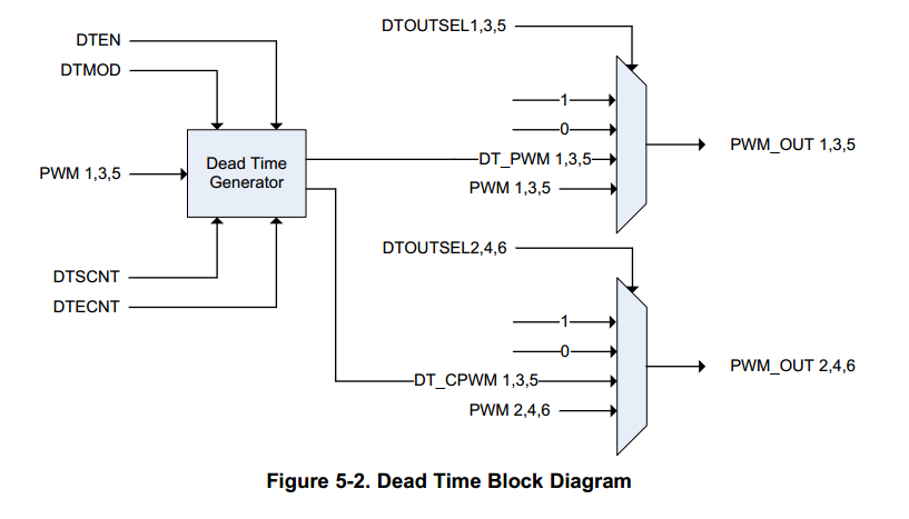
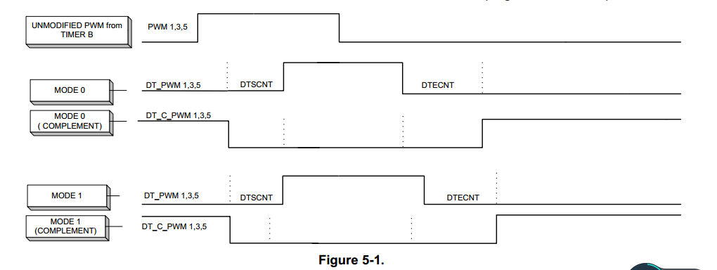
Tool/software: Code Composer Studio

Hi Team: my MCU is DRV91680.
DTCTL = 0x01;

DTCNT = 0x7F7F;

According to this configuration, the PWM output waveform has only one side of the dead band. What's the problem?

  • Hi:

         My MCU is DRV91680.

         I found the following problem in debugging:

         Dead Time Control (DTCTL)

         Dead Time Count   (DTCNT)

         Dead Time Output  (DTOUT)

          I configured as follows in the program:

          DTCTL = 0x0001;

          DTCNT = 0x7F7F;

          During debugging, it is found that the PWM complementary waveform has only one edge (the rising edge / falling edge) of the 5uS, but DTCNT, I have all configured the same clock count.


  • Can no one help me?
  • Weiwei,

    1. From your setting (DTCNT = 0x7F7F), I expect you'll see the same amount of dead time on both the rising edge and the falling edge.
    2. How is your DTOUT configured?
    3. Do you have a waveform that you can show - please take the measurements at the pin?

    Regards,
    James.
  • Weiwei,

    1. I can see your scope shot now. CH2 (green) is the low side gate and CH3 (blue) is the high side gate.
    2. It looks like your frequency is 20kHz with 40% duty cycle.
    3. The issue is at the LS turn-on/HS turn-off transition. We will have to understand how your gate driver is designed - there is potentially some imbalance in your turn-on/turn-off transition.
    4. You can send me the schematics privately for feedback.

    Regards,
    James.
  • James,
    1.My design intent is: PWM1 3 5 PWM2 4 6 to produce complementary output waveform output pin (with a double edge, but the dead) configuration register can only get single edge dead, the other side will lead to the upper and lower tube to wear MOS.
    2.DTOUT =0x0040 .
    3.Is the chip address mapping problem causing the register configuration to be invalid? I see in the program (.Map) file that DTCNT_H is 0x00000542 and DTCNT_L is also 0x00000542. In the (.Map) other program style, DTCNT_H is 0x00000543
  • Weiwei,

    1. The map you described will cause DTCNT_H not to be written.
    2. Correct map: 00000542-DTCNT_L and 00000543-DTCNT_H. You can verify you've set the DTG correctly by checking the registers in CCS debug window.
    3. Please make sure you're working off the lastest SDK.

    James.

  • James,
    1. I don't have the latest SDK, I only have Feb 12, 2014 SDK.
    2. Can you provide me with the latest SDK?

    (Chinese TI technicians have replied to me that technical support for DRV91680 is currently available only
    at the TI headquarters in the United states.)

    My mailbox: 837670176@qq.com

    Thank you very much.

    Regards,
    Weiwei.