Because of the holidays, TI E2E™ design support forum responses will be delayed from Dec. 25 through Jan. 2. Thank you for your patience.

This thread has been locked.

If you have a related question, please click the "Ask a related question" button in the top right corner. The newly created question will be automatically linked to this question.

DRV8353R: Paralleling MOSFET / Power Losses / Shunt

Part Number: DRV8353R

Hy

My First Time Design Questions are:

1. Is it possible to place two MOSFET's in parallel? (See attached schematic screenshot of on Phase Leg)
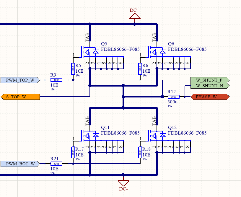
2. The thermal information are confusing. What is the maximum power dissipation of the gate drive section?

The conditions are: Tamb= 75°C, fs = 12kHz, Vgs = 15V Qgmax = 180nC (2xQg of 90nC),  Independent PWM Mode, Space Vector sinusoidal control

3. "Standard" applications requires a gate resistor for each MOS. Is this also true for the DRV8353R?

4. Is it possible to use the internal current shunt amplifiers in a "phase current configuration" instead the "leg current configuration"

5. Is Figure 33 the only dead time insertion mode?Can we disable the dead dime feature?

Kind Regards

Rolf Lerch

  • Rolf,

    1. Yes parallel FETs are fine, what is the reasoning for doing this in your design? I just want to understand the need.
    2. We do not specify a maximum power dissipation unfortunately.
    3. The DRV835x does not require gate resistors as it has Smart Gate Drive, you can view info here: https://www.youtube.com/watch?v=lUzQybOTTmU
      1. This being said, when parallel FETs are used, gate resistors are recommended as not every FET is the same and often we need to balance parasitics between two FETs. If one of the parallel FETs were to turn on slightly before the rest and gate resistors were not installed, there may be ringing and oscillations as the FETs fight for charge.
    4. This is not recommended and will likely damage the CSA. Our CSA are cannot handle the common mode voltage required for in-line phase operation. If needed I can recommend an external INA that could accomplish this.
    5. Dead-time is automatic in all modes and operations except Independent mode, you can read about this in section 8.3.1.1.4.

    Regards,

    -Adam

  • Hi Adam

    Thank You for the quick response. It helped, but I still have some questions

    1. The answer is simple: Power. We need do deliver 4kW for an low rpm motor -> continuous current of 90Arms. We did not find a single MOS solution for this

    2. No power rating is OK for me. but wher does the 

    3. I already saw this promo video. Unfortunately they do not show our paralleling problem. The ringing/Vgsth problem is known. But I do not know how to proper design the resistor values. Any recommendation?

  • Remark / Addon to #2.

    2. No power rating is OK for me. but where do the 26.6°C/W come from in EQ.39? And why do you not take account of the internal LDO losses (Chapter 8.3.2) in the total power losses calculations (chapter 9.2.1.2.6)

    DRV835x Losses.xlsx

  • Remark / Addon to #5.

    That is fine we will use our own control with the TMS320f28377. We usually design an MOSFET power stage with individual date resistors On/Off to turn on slow and turn off fast the switch. Is this possible withe the DRV835x ?Can we set the charge and discharge current individually?

  • Rolf,

    1. Understood, just wanted to make sure.
    2.  The 26.6 is RthetaJA, this is from the packaging team. This is generic for the package. Which LDO are you asking about?
    3. I would start with 5-10 ohms and then adjust from there based on the Gate-to-source voltage you are seeing at turn on/off. If using the H device (hardware control) then the IDRIVE is fixed at a 1:2 ratio, sink is 2x of source, but it is fully adjustable. If using the S device (SPI control) then the source and sink are independent and can be controlled in any ratio. Since you are using gate resistors, this may allow you to have a more simple BOM, use the same resistors for all FETs but still control the source and sink independently without a seperate diode path and second resistor.

    Regards,

    -Adam

  • Hi Adam,

    I'm talking about the DVDD Regulator in chapter 8.3.2. Did you check my calculations in DRV835x Losses.xlsx? There it's the Pdvdd value in Line28

    Regards

    Rolf

  • Rolf,

    I have asked the team and will get back to you this week.

    Regards,

    -Adam

  • Rolf,

    Sorry for the delay. The reason why DVDD is included in equation 1 but not in section 9.2.1.2.6 is because equation 1 is only valid if DVDD is used to drive external loads. These external loads would be additional losses which are not included or assumed in section 9.2.1.2.6.

    Section 9.2.1.2.6 includes the internal DVDD losses since they are derived from VM and IVM is included.

    Obviously higher voltage (VM) systems should not use the DVDD output externally as the LDO is not very efficient for driving external loads.

    Regards,

    -Adam