This thread has been locked.

If you have a related question, please click the "Ask a related question" button in the top right corner. The newly created question will be automatically linked to this question.

DRV8303: DRV8303 drives MOS current down

Part Number: DRV8303

Hi,Ti

Now I am using DRV8303 to drive INFINEON MOS model 028N06NS.

During debugging, it is found that the drive is normal when no load is carried. When load or motor is blocked, the current cannot be added and abnormal sound occurs to the motor, and the blocked current is 0.9A.
It is powered by a 24V lithium battery.

The brushless hall reduction motor has a motor power of 180W and a speed of 2000RPM, and the shaft output speed after reduction is 120RPM.

The attachment is the peripheral circuit of DRV8303. Could you please help to analyze it and see what the problem is?

Problem phenomenon supplement:

1) Control Register 1 is set to 0x1610 and Control Register 2 is set to 0x1804

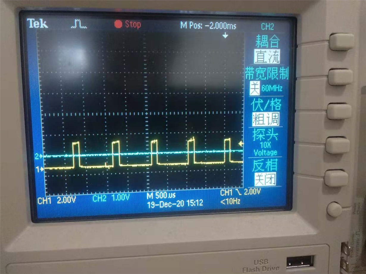
2) When problems occur, the nFAULT pin outputs the periodic signal in the diagram, and the nOCTW pin is always at a high level

3) The pins of DVDD, GVDD and PVDD were observed with oscilloscope without obvious voltage sagMOS028N06NS.pdfDRV8303外围电路.pdf
  • Hello Dominic,

    Comments on your data

    The Fault table shows that DVDD, GVDD, and PVDD UVLO (and GVDD OVLO) are the ones responsible for nFAULT = 0b1 and nOCTW = 0b0. Your register settings don't look like they would change the behavior shown in the fault table. You have said that there is no obvious dips in those voltage during this operation which contradicts the fault table. As a result I encourage you to move the ground lead attached to the oscilloscope so it is close to the GND pin of the DRV as you can and repeat the process while capturing nFAULT, nOCTW, and <signal> (PVDD, GVDD, etc). This will ensure there is nothing wrong with probing techniques.

    Other troubleshooting

    In parallel, the rise of nFAULT is being cleared rapidly and periodically. Does the nFAULT signal match up with any signal on the device? I can't tell what the horizontal time division in the scope shot is (500us per division maybe? So the signal repeats approximately every 1 ms or 1kHz? 1kHz could be a PWM frequency or the speed of the motor, etc).

    Other comments:

    I've seen similar stalling conditions causing damage to GVDD. Specifically, the stall condition will result in a surge in current to the motor, which couples into the gate low side pin and sends energy back into GVDD and damages the rail. This is solved with lowering of the overcurrent tripping point and verified by using a DMM and checking the impedance between the GLx pins and the GVDD pin. So I would prioritize verifying if that is the case.

    Best,

    -Cole

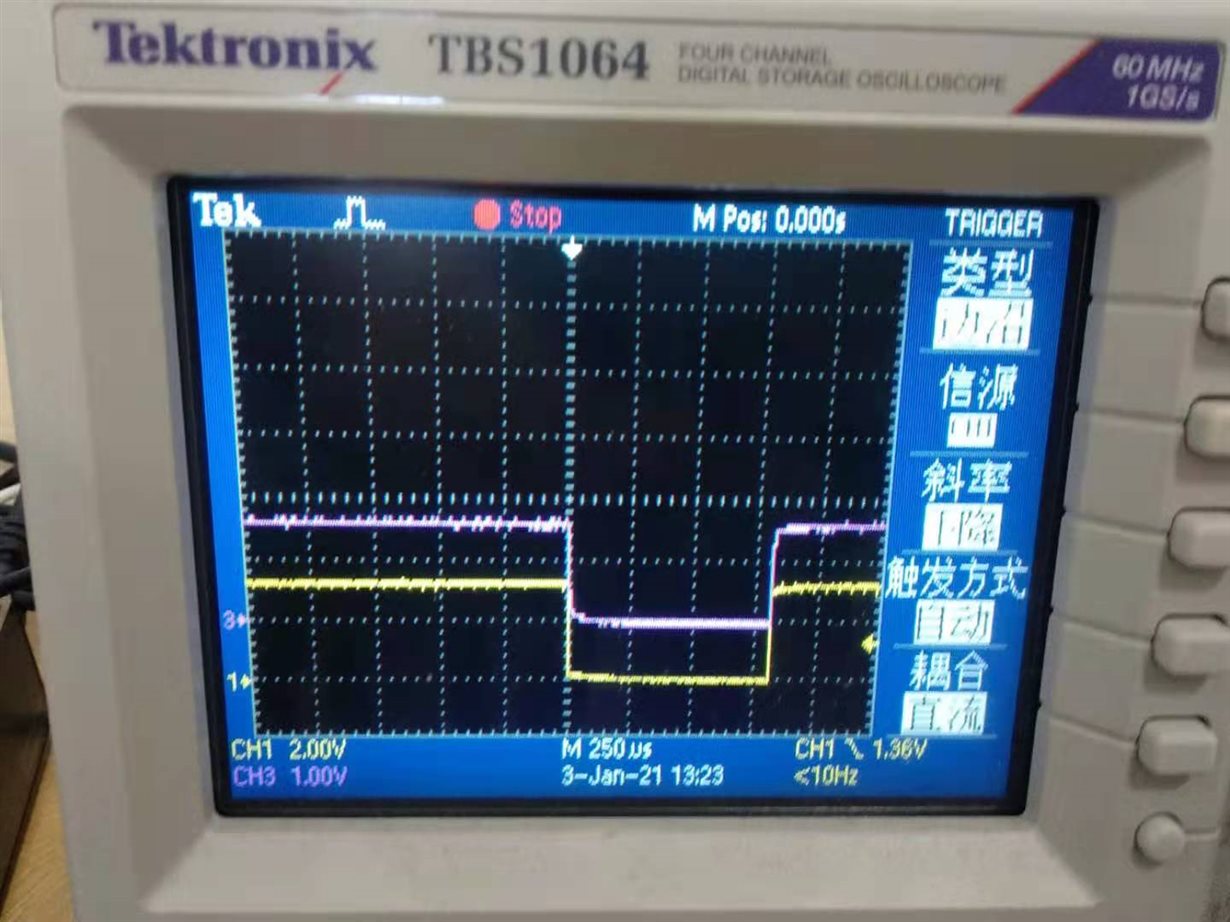
  • Hello Cole , the horizontal time division in the scope shot is 500us per divsion, and the PWM frequency is 20kHz. Maybe there is no relationship between them. When nFAULT pin is low, I read the status register1 and status register2. The status register1 is 0x0000.The GVDD_OV bit is 0b0. 

    And when  nFAULT pin is low,  The SO1 pin of the amplifier output is also low.

    The yellow line is nfault pin. The pink line is SO1 pin.

     So I think the fault is DVDD under voltage, but I don't know how to deal with this fault. Can you give me some  suggest?

    Best, 

  • Hello ,

    That you for correlating the nFAULT signal with output of the amplifier.

    Can you check AVDD with an oscilloscope and see if its following the operation? The CSA is supplied by AVDD.  

    I'm also noticing that the AVDD output isn't tied to the fault table, I'll check this in parallel. 

    Best,

    -Cole

  • Hello Cole ,

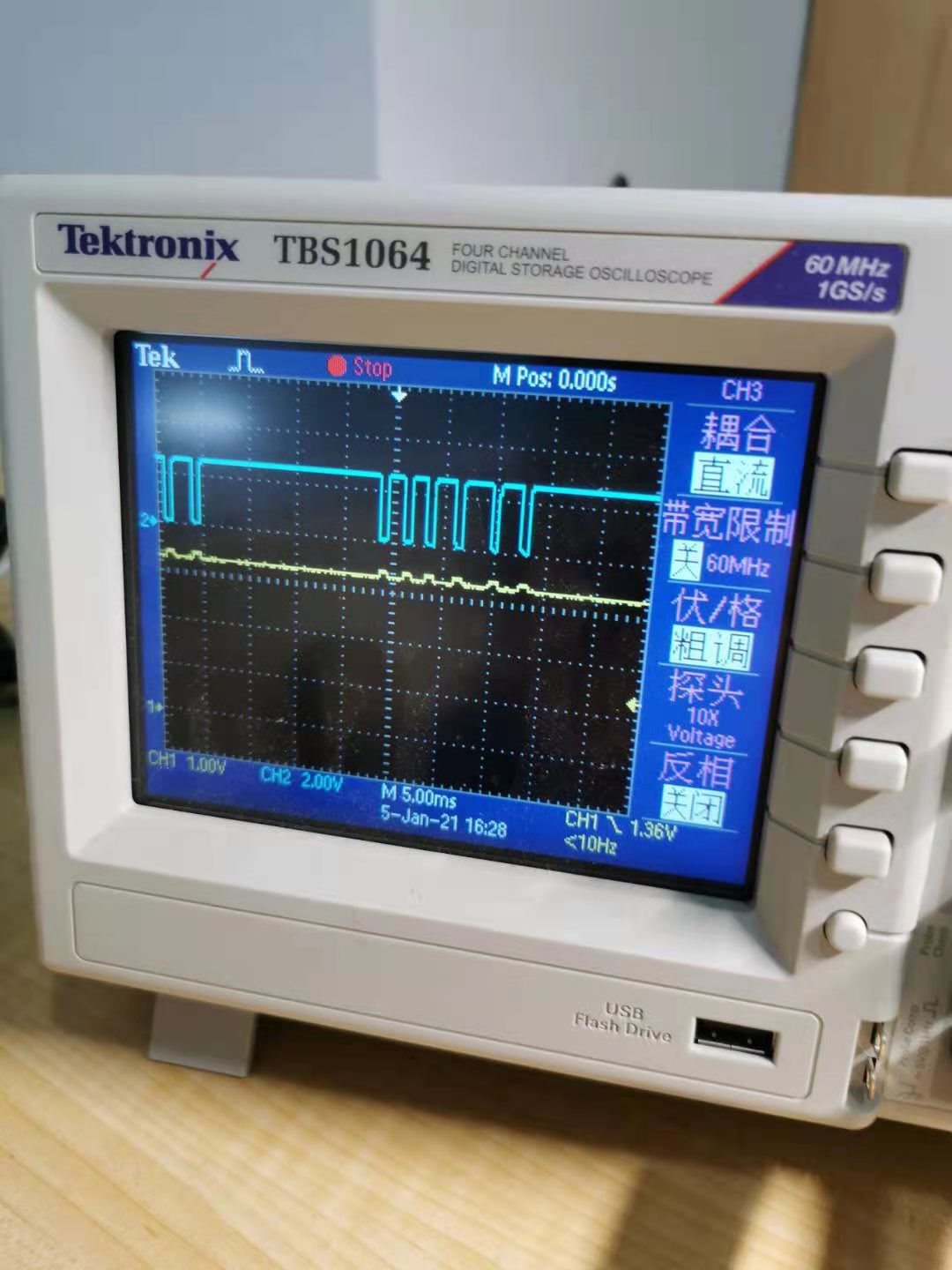
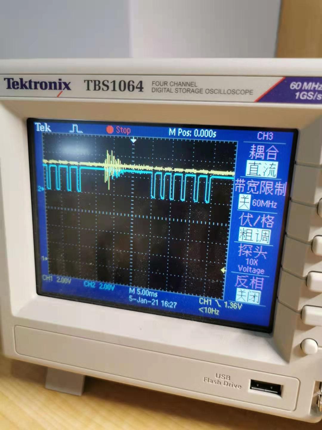
    According to what you said,I have moved the ground lead attached to the oscilloscope close to the GND pin of the DRV8303, but the pins of DVDD, GVDD, AVDD and PVDD are still observed with oscilloscope without obvious voltage sag when the nFAULT pin is low.

    The picture below is the pin of AVDD and nFAULT. The blue line is nFAULT, the yellow line is AVDD.

    The picture below is the pin of GVDD and nFAULT. The blue line is nFAULT, the yellow line is GVDD.

  • Hello ,

    Yes, it looks like the rails are stressed with nFAULT is not asserted so its clear there is some sagging when the device is trying to operate normally. Because these rails are generated by the device, there's not much to be done. As a result, the root cause usually falls upon 1 of 3 reasons.

    Please excuse the formatting, the formatting box is near worthless when trying to make the post look a bit better.

    1. The device was damaged or partially stressed during operation

    This could be ESD or too high of gate drive current (GATE_CURRENT) for the QGD of the FETs used. 7nC for those FETs is very small, I suggest you read this blog post and make the GATE_CURRENT setting lower than what is calculated: https://e2e.ti.com/support/motor-drivers/f/38/t/796378

    This is pretty uncommon for this device in particular

    2. The assembly was done incorrectly.
    This is usually caused by poor contact with the Die Attached Paddle Thermal Pad on the DRV to the PCB thermal pad footprint. This leads to large paraisitics for current traveling by the thermal pad and introducing noise. Sometimes, this also leads to poor connection on a pin or series of pin related to regulators.
    This is pretty common for those who did not use an expert PCB manufacturer to replace or assemble the PCBs. For example, a non-manufacturer needs to use a solder wave reflow machine or a "board warmer", heat gun, and a sufficient amount of solder paste so that the solder doesn't flow through the thermal vias and not collect on the bottom of the thermal pad
    3. Poor Layout
    Specifically, the GND'ing around the device and the gate driver. Long GND loops, cross talk from other switching signals, not enough GND stitching vias are usual suspects here.
    This is pretty common for those just getting started with or who are new to gate driver designs

    We have a post leading to an app note that helps demonstrates good techniques: https://e2e.ti.com/support/motor-drivers/f/38/t/746299

    Best,

    -Cole

  • Hello Cole,

    Thank you for your  advise. I will redesign the PCB and retest the circuit board.

    Best,

    -Guoqing Huang