Other Parts Discussed in Thread: CSD18540Q5B, CSD18533Q5A
hi TI :
i have 4 question needing help:
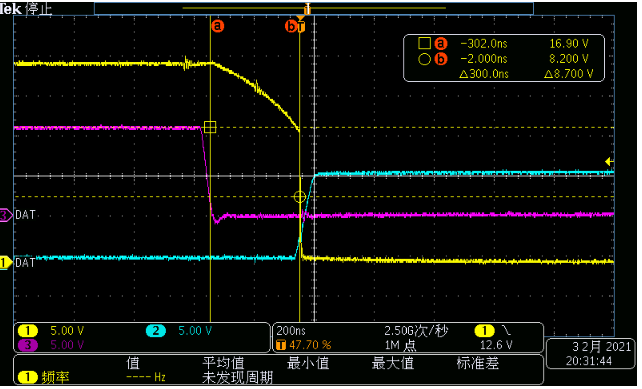
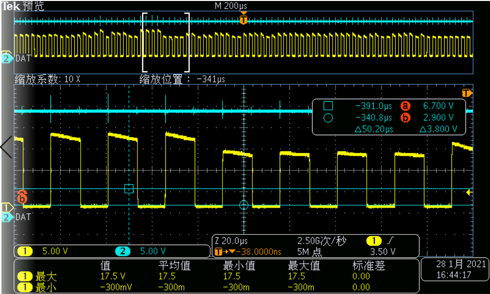
#1: Low-side gate drive voltage,it vary from 11V to 15V , as the datasheet refer that the voltage is fixed at 11V , so why ?
check the waveform YEL: low side drive voltage BLU: VM voltage
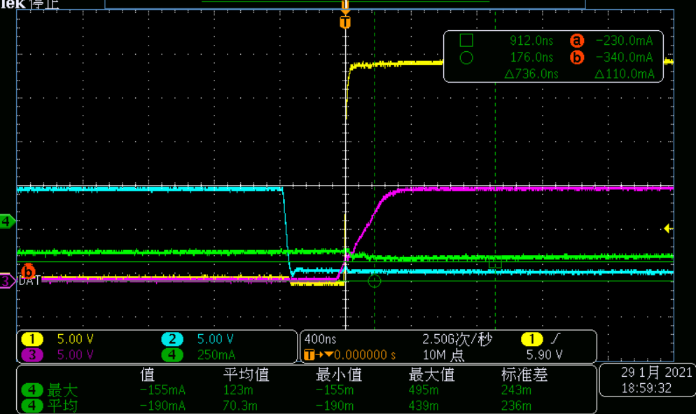
#2: High-side gate drive voltage,it vary too,check the waveform

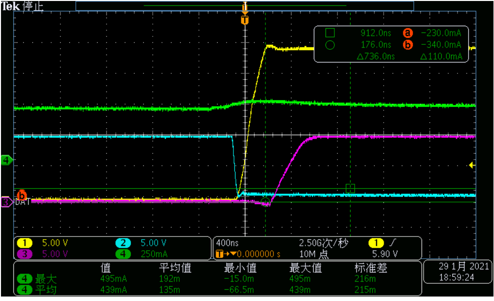
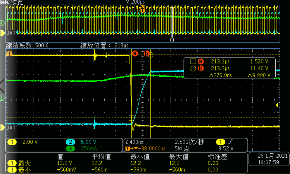
#3:the MOS Drive Rising edge oscillation ,how to solve the problem as I have set the register IDRIVEP_LS and IDRIVEN_LS to 0000b, the drive current is also smallest ;
check the waveform

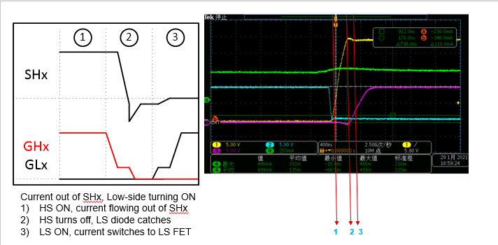
#4: the high side -MOS close delay long,how to solve ?
we also use TI-MOS -model : CSD18540Q5B
#5: the following is our schematic ,pls check and share some suggestions