This thread has been locked.

If you have a related question, please click the "Ask a related question" button in the top right corner. The newly created question will be automatically linked to this question.

DRV8303: False over current faults

Part Number: DRV8303

No load connected with proper threshold settings and yet over current faults chatter at the digital output. Increased the threshold but had minimal effect. Dead time is large and increasing it is not helping much either. What could be wrong? When the function is only disabled, it works fine. There are 10Ohm gate resistors.

Thanks.

  • Hi Mason,

    The OCP works by measuring the VDS of the FET. Can you please take scope shots of FETs while switching to see when the VDS might be exceeding the thresholds you set for the part? This may be due to slow turn-on time for the FETs rather than a shoot-through condition. What is the your setting for GATE_CURRENT in register 0x02? Can you increase it?
  • Thank you, James for your reply. The gate current was supposed to be maximum but we are not sure of our register setting. We are in process of verifying it. Meanwhile, would you be able to provide us an alternate hardware method to disable the gate signals without shutting down the SPI bus. Our firmware team is not happy with the Gate_Enable pin killing their SPI link with the chip.
  • Hi Mason,

    Are you using 3-PWM or 6-PWM mode?

    If you set the device to 6-PWM mode, then assert a low signal on all the INxx pins, this will make the gate outputs low and will Hi-Z the FET bridges. Is that acceptable?
  • Thanks, James for your response. Per customer requirements, the bridge needs to be disabled by hardware in addition to MCU deactivating the gates signals, in two independent places. The gate signals are being blocked by a tri-state buffer as the first method and for the second, the enable pin of the DRV chip was being used until firmware said no! Their SPI bus was also dying with it, which wasn't acceptable. I was thinking of opening the boost cap...

  • Mason,

    I'm not sure I completely understand your setup. Was my suggestion helpful?

    If your MCU has a high-Z condition on the pins that control the INxx pins, all the H-bridge FETs will be disabled. The INxx pins have internal pulldown resistors, so the H-bridge should be shutdown by default.

  • James,

    This is totally independent of firmware and MCU. Pure hardware controlled by customer safety systems should be able to shut down the bridge at two locations. MCU will be only notified to Hi-Z the pins but that's not enough for the customer. Do you think if I open the boost cap, it will kill the gates? Any other ideas?

    Thanks,
    Mason
  • Mason,

    I don't think it's a good idea to put anything in the path of the charge pump cap because it's sensitive circuitry. Maybe you can short GVDD to GND to engage the device's protection UVLO for the GVDD. We don't intend the device for this operation, but it's something you can try.

    What is the issue with using the EN_GATE pin as you originally did, but reloading the registers after the customer's safety condition clears?
  • After talking to a colleague, I take back my comment about shorting GVDD. We do not recommend doing anything to the charge pump.
  • James,

    I assume the resulted GVDD_UV condition from shorting the GVDD to ground (while PVDD is full on) will still let the SPI going unlike PVDD_UV that kills it. In that case, we're back in business.

    Firmware complains that customer safety locks could be engaged at start up. Therefore, there should be a dedicated state machine that doesn't do anything other than (re)initializing this chip based on convoluted conditions/timing of these locks during/after startup and operation. I'm still haggling with them but no luck so far.

    If shorting the GVDD_UV to ground is safe for the chip and reliably disables the gates while SPI is still going, then we're getting somewhere.

    Thanks,
    Mason

    PS) Haven't heard back about the gate current fix for the short circuit chattering yet. Will let you know soon.
  • Alright, I got it. I have to find a different way...
  • Mason,

    The only other thing I can think is to put transistors or buffers on all the INxx pins to pull them to ground or open the path from the MCU (relying on the internal pulldowns) when the particular safety condition happens.
  • Thanks, James. This is already done as the first method.

    The second one is still under investigation and I think I found a solution.

    Still waiting for the SC chatter results to close this ticket.

    Mason
  • James,

    Getting back to the false short circuit faults from the chip, it's only happening on high side devices. I'm going to get some scope captures of the gate voltage across the gate resistor that should tell us what the gate current looks like. Firmware team adamantly believes that the gate current is set to maximum.

    FETs have also external Schottky diodes in parallel to them. Also the 5 pins for phase-C FETs (pins 30-34) are left open.

    Thanks,

    Mason

  • Mason,

    If you don't use phase C, do you keep the INxC pins low? Do you use 3-PWM or 6-PWM input mode?

    When you read the fault register, do you see OCP faults on the C phase or do you only see them on the A and B phases?

    The OCP works by measuring the voltage across the FETs. For the high-side FETs, this measurement is between PVDD and SHx. While I'm interested to see the gate signals, I'm mainly interested in the voltage across the FETs. If you can use differential probes to measure the voltage from the FET drain to source, that will help to find the cause of OCP. What is the value you program in the OC_ADJ_SET bits? The OCP will trigger when the voltage across the FET is above this threshold for at most 1.5 us.
  • Hi James,

    INxC pins are both held low and its driver pins are left open.

    6 PWM mode inputs.

    OCP faults appear only on phases A and B high side devices.

    OC_ADJ_SET value is currently 0x19H and doubling it improved it slightly.

    I will capture the gate and drain-source voltages hopefully today.

    I'm going to also run some scenarios with different OC_ADJ_SET and GATE_CURRENT values.

    So far all tests have been done with the bridge output unloaded (open load). However, we run motors with it successfully when we disable the OCP fault.

    If you have other scenarios in mind, please let me know. 

    Thanks,

    Mason 

  • James,

    A question about the GVDD_OV fault, basically when PVDD hits around 64V, this fault will be set (16Vth - 12Vg@60V). Correct?\

    Thanks,
    Mason
  • GVDD should should regulate around 11-V. If somehow it becomes 16-V or greater, the device will shutdown. I don't think it protects PVDD directly.
  • Thanks, James. That "somehow" is everybody's question right now! How can it rise to 16V? What has to go wrong?

    Regards,
    Mason
  • Mason,

    The example the datasheet gives in 7.3.3.4 is the charge pump capacitors or GVDD capacitor shorting to an external voltage higher than 16 V. This kind of condition completely shuts down the chip, and it can only be reset by toggling the EN_GATE pin. If this kind of fault condition occurs, something conductive may be laying across the board and the board should be inspected prior to using again (section 7.4.1).

  • James,

    We just noticed that if we program the control registers while PWM is running, the chip's behavior becomes unstable until the transmission is complete.

    In other words, as the bits stream into the control shift register, the settings associated with each bit toggle per the shifted data in real time.

    Are the control registers buffered? Should we avoid programming the chip while PWM is running?

    Thanks,

    Mason

  • Mason,

    Which bits in the control register are you trying to change? What is your SPI clock frequency compared with your PWM frequency? In your end application, is there a reason you need to change these settings while driving?

    Because the control registers control the gate driving features in the device, I wouldn't change their settings while actively toggling the device.
  • Mason,

    How the SPI input handles data is mentioned in section 7.5.1.1 in the datasheet:

    "While SCS is low, at each falling edge of the clock the new input word is sampled on the SDI pin. The SPI input
    word is decoded to determine the register address and access type (read or write). The MSB will be shifted in
    first. Any amount of time may pass between bits, as long as nSCS stays active low. This allows two 8-bit words
    to be used. If the input word sent to SDI is less than 16 bits or more than 16 bits, it is considered a frame error. If
    it is a write command, the data will be ignored. The fault bit in the next SDO response word will then report 1.
    After the 16th clock cycle or when nSCS transitions from LOW to HIGH, the SDI shift register data is transferred
    into a latch where the input word is decoded."
  • James,

    Firmware is writing the same word into the control registers every 1ms while PWM is running, which is wrong and it's getting fixed. However, I'm clearly seeing on the scope that the gate current is changing on the fly while PWM is running, which means that either the shift register is not buffered/dumped at nSCS transition, or the control word is changing every time. Either way, we are getting somewhere...

    Thanks,
    Mason
  • Mason,

    Could you please share this scope shot with me?
  • James,

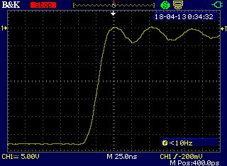
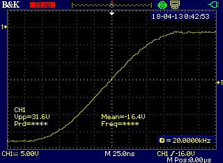
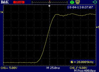
    Here are the three that I captured happening on a pseudorandom basis on the top side drain-source voltages as the control register is being updated at 1ms rate.

    As you can tell they represent all 3 gate current settings of 0.25A, 0.7A and 1.7A for a 50nC gate charge.

    Thanks,

    Mason

  • Mason,

    Thanks for the scope shots. I'm wondering when this happens in relation to when the data is written by the SPI. If the gate current changes after the SPI transaction happened, then you may be seeing the gate current change as the new data is clocked into the register.

    As an applications engineer, I'm not sure on the internal working of the device. If you would like me to investigate this with my design team, could you take a scope shot showing the traces you show above and the SPI signals (SCLK, nSCS, and SDI)?
  • Thanks, James for your support so far.

    We have stopped updating the device altogether and just program it at startup and every time we need to clear a fault. The behavior has improved significantly but full investigation is not possible yet (coding isn't complete).

    I'll do my best to capture the SPI signals as well...

    Regards,

    Mason