Other Parts Discussed in Thread: CSD19532Q5B
Hi
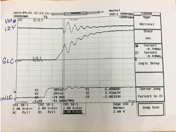
I am using the DRV8350RH chip. VM and VDRAIN are not tied together. VM is generated via a DC regulator from VDRAIN.
Are there any timing sequence requirement among VM, VDRAIN and ENABLE? By the way, the ENABLE pin requires an external power to pull up high before the chip can function.
Also, why is there a maximum pulse width requirement on ENABLE pin to reset the driver chip, can we keep the ENABLE pin low longer than the maximum pulse width?
In the last six months, we have burned up 10 of DRV8350RH chips. Some of them may due to higher biasing of IDRIVE/VDS, but others simply lost VGLS over time. What can we do to prevent lost of VGLS? VGLS will drop down to 3.8V when it failed.
Regards,
Candy