This thread has been locked.

If you have a related question, please click the "Ask a related question" button in the top right corner. The newly created question will be automatically linked to this question.

DRV2700: Getting damaged with high supply current

Part Number: DRV2700

I am having troubles making the DRV2700RGPT work.

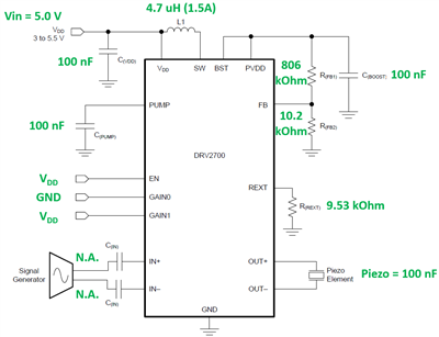
After successfully using the DRV2700EVM for my application, I have designed my own PCB and let a professional PCB manufacturer assemble it. I have used the layout from the DRV2700 Datasheet (Figure 22, values of components below).

EN has been fixedly programmed at “1”, Gain = 38.4 dB, V_PVDD = 105V.

First, I connect the piezo. Then I connect the input signal (differential, from a AC signal generator). Then I connect the power. In this sequence. I believe I have already damaged 3 PCBs.

In the first trial, I managed to measure V_FB = 1.15 V and V_BST = 105 V. The quiescent current from the power supply was 72 mA when input signal was muted, and around 230 mA, when input signal was maximum. I managed to make this work for a few minutes. But when I connected a different piezo to the output, the quiescent supply current surged to 500 mA (limited by my power supply) and no output was generated. Since then, I was not able to make this circuit work again and the 500 mA is always there, so I disconnect it quickly.

Can you please tell me what is the problem with my design?

I have read the DRV2700EVM datasheet as well, and all the E2E Forum replies, but I can’t find the right answer.

Please let me know.

  • Hey,

    Based on your schematic nothing seems to be wrong to cause the problem you are describing. 

    I will need a few more details regarding the voltages at different nodes when this 500 mA is running through, to determine if the chip is fried. What is the boost voltage? the voltage at SW pin? and is there any voltage at output when is piezo is not present?

    Are all three boards doing the exact same thing as you described in the first?

    The problem is most likely due with the layout and component arrangement on your board or possibly the piezos you are using. If you have any more undamaged boards I might try putting a capacitor at the output in stead to see if that shows different behavior or results. 

    Maybe try referring to layout guidlines under section 11 of the DRV2700 datasheet for reference to compare your PCB layout

    Best,

    Carson Allen

    LPAA Applications

  • Dear Carson,

    No, the 3 boards do not behave in the same way. Here are my measurements results:

    Board

    I

    II

    III

    I_q (mA)

    28

    500

    500

    V_FB (V)

    0.05

    0.25

    0.30

    V_BST (V)

    4.3

    10.5

    13.3

    V_SW (V)

    5.0

    2.8

    2.8

    V_OUT (V)

    0

    0

    0


    These are my design details, according to the layout guidelines from the datasheet:

    Thermal pad and GND are correctly connected.

    Resistors RFB1/2 are 1.5mm away from FB pin.

    All PCB traces are 0.25mm wide.


    I still cannot find the cause to the circuits not working.

    Please assist.

    Regards.

  • Hey Again,

    I am going to discuss this issue your facing with other members of my team and get back to you with a recommendation soon

    Best,

    Carson

  • Hey,

    Can I see the full PCB layout of your design instead of just the schematic that you have at the top?

    Best,

    Carson

  • Hello Carson,

    Yes you can, but I cannot post it publicly. Please drop me an email.

    Thanks!

  • I sent you correspondence through the email on your profile