This thread has been locked.

If you have a related question, please click the "Ask a related question" button in the top right corner. The newly created question will be automatically linked to this question.

DRV8323: DRV8323S

Part Number: DRV8323

Hello TI team,

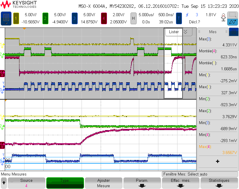
We are using the SPI interface to communicate between our microcontroller and the gate-drive DRV8323S. We followed your hardware recommendations described in the datasheet by using only a 10k pull-up resistor connected to the SDO pin. We record a slow rise time on SDO around 600ns.  

There's no capacity in parall. What's your opinion?

Channel C1 : Chip Select

Channel C2 : SDI

Channel C3 : Clock (560kHz)

Channel C4 : SDO

Pierrick Ecoeur

pierrick.ecoeur@sonceboz.com

  • Hello Pierrick,

    It looks like the picture was not loaded correctly. Could you save the picture and use the import function instead of copying and pasting directly into the reply box if the below answer is not sufficient?

    Short Answer,

    I'd recommend experimenting with a lower value pull up resistor as there is no concern for doing so. This should decrease rise and fall time on the line. 

    Longer Answer

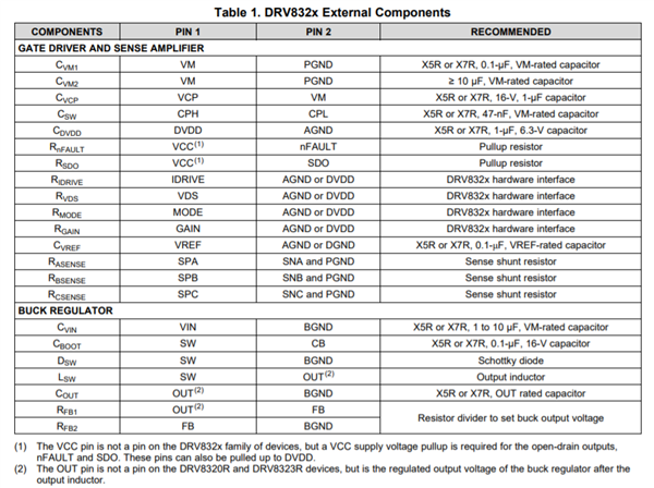
    The recommended components in table 1 of the datasheet signify a "pull up resistor" (as shown below). This is the allow user flexibility and acknowledge that other factors will contribute to rise and fall time on the line. The application section shows 10k ohm, but this is a recommended starting point based on our EVM and prototype designs we made during development.

    The rise and fall times of a signal are determined by the equivalent pull up resistance (R), and the equivalent capacitance on the line (C). Thank you for noting that there is no external capacitor in parallel, but the equivalent capacitance also depends on parasitic capacitance. This could come from trace length, wire length, component footprints, MCU I/O, and DRV I/O structure. 

    The dominant components in the parasitic capacitance is the I/O structure of the MCU and DRV. Because we can only predict the DRV I/O structure we can generalize the range of pull up resistance is needed. Since we cannot predict the MCU's IO structure we acknowledge that parasitic capacitance might be lower or higher based on the I/O topology and process.

    In general, most users will try some value of pull up resistor, and increase it or decrease based on the waveform. Equivalent capacitance could be modeled in a SPICE simulator, along with the pull up to see the predicted rise time, but most decide to look at the waveform, change the resistor value, change the BOM, and replace the values on their existing boards.

    Best,

    -Cole

  • Hi Cole,

    Thank you for answer.

    I import the picture below with a 10k pull-up resistor.

    I repeat the test with a lower pull-up resistor, 1.5kOhm, see below the picture. The rise time is reduced around 90ns. 

    The I/O capacitance of our MCU is given around 5pF and the trace lenght on the PCB is less than 20mm. Do you know the parasitic capacitance of the internal gate-driver?

    A trise of 90ns seems to be OK?

    Best regards,

    Pierrick

  • Hello Pierrick,

    I can go check out the capacitance of our device if you'd like, but it looks like you've got the data you require.

    Essentially, the SDO line would take more than half a clock period to rise to the final value with the 10k ohm, where the second picture shows that that SDO reaches its final value before the half way through the high time of the clock transition (or before half the clock period), which is much better (and "OK" from a data integrity point of view). Which means, you could leave it 1 kohm with no issue.

    The general advice I can give you, if you run into open drain digital outputs again, is that you should try to use the largest pull up resistor you can, without sacrificing data integrity. This is because the open drain output holding the signal low, means there is current flowing through the pull up resistor (burning energy).

    Data integrity is usually defined by the protocol you are using. For example, I2C might require the voltage of the signal to within 33% of the intended 1 or 0 some time (say, 10ns) before the edge of the falling clock signal. I do not know the SPI protocol on hand, but I assume there is some t_hold and logic high or low values that are required to successfully read a 1 or 0 on the communication line. I used the "signal reaching final value within 1/4 the clock period (or 1/2 the clock high time)" as a rule of thumb based on experience.

    As such, you can go look up the SPI communication and understand the parameters required and increase the resistor to determine the optimal theoretical resistor. Or, you have the board and code, you can swap it out and look at the waveform and see if the transaction was successful.

    Best,

    -Cole