This thread has been locked.

If you have a related question, please click the "Ask a related question" button in the top right corner. The newly created question will be automatically linked to this question.

CCS/DRV8803EVM: How to control the output of the DRV8803EVM using a PWM output from the EK-TM4C1294XL

Part Number: DRV8803EVM
Other Parts Discussed in Thread: DRV8803, EK-TM4C1294XL, , DRV8804EVM

Tool/software: Code Composer Studio

Hello,

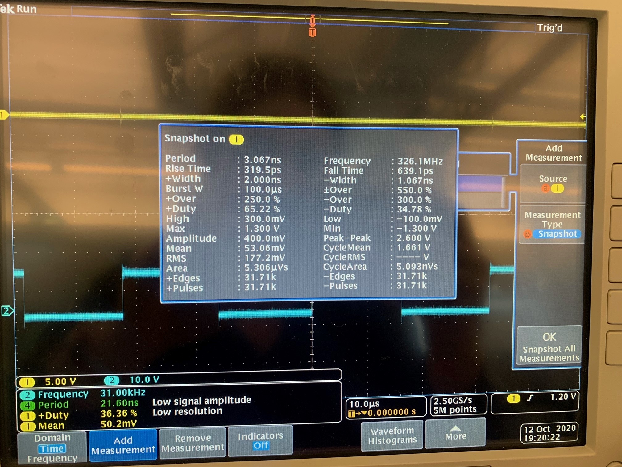
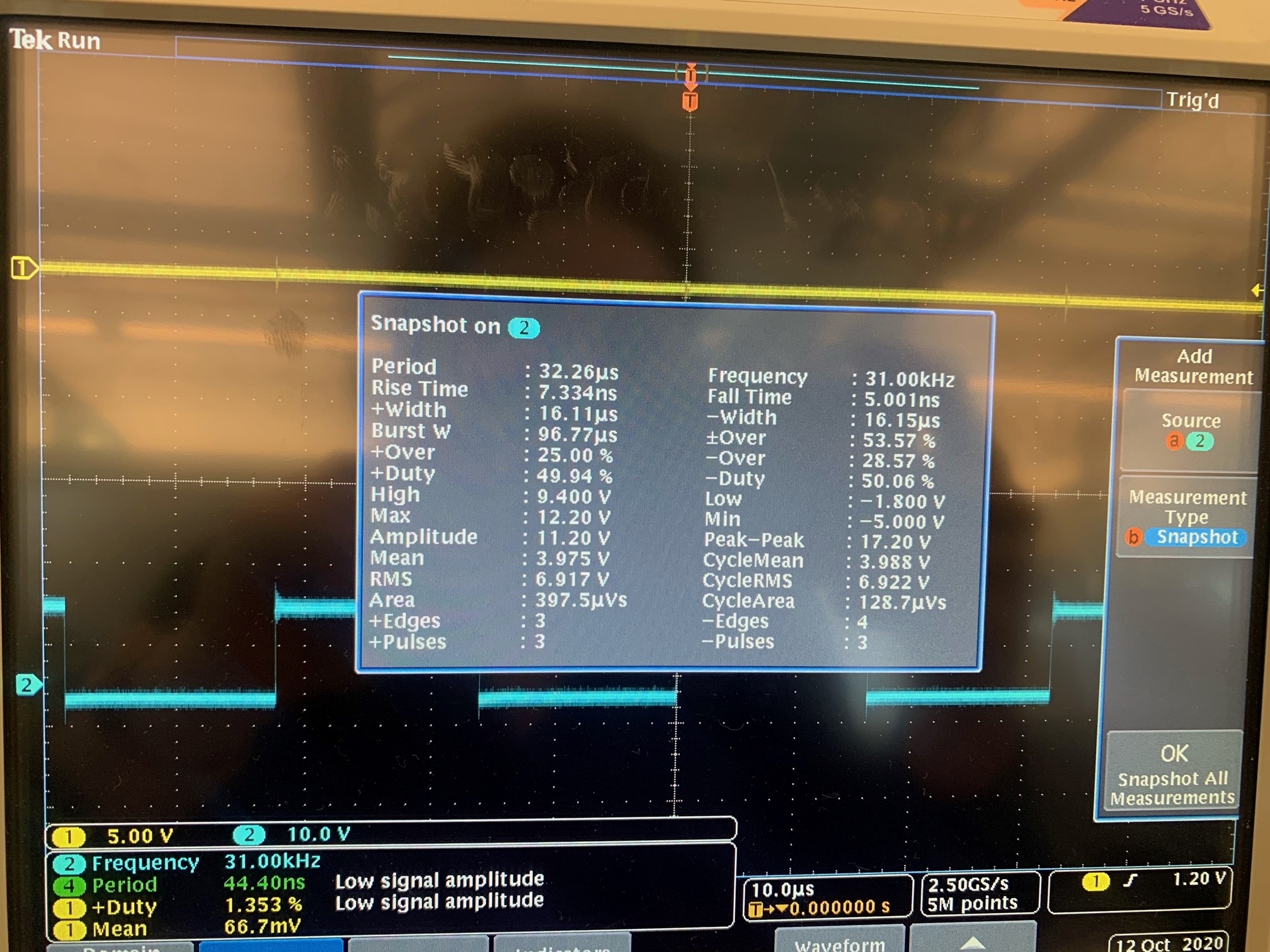
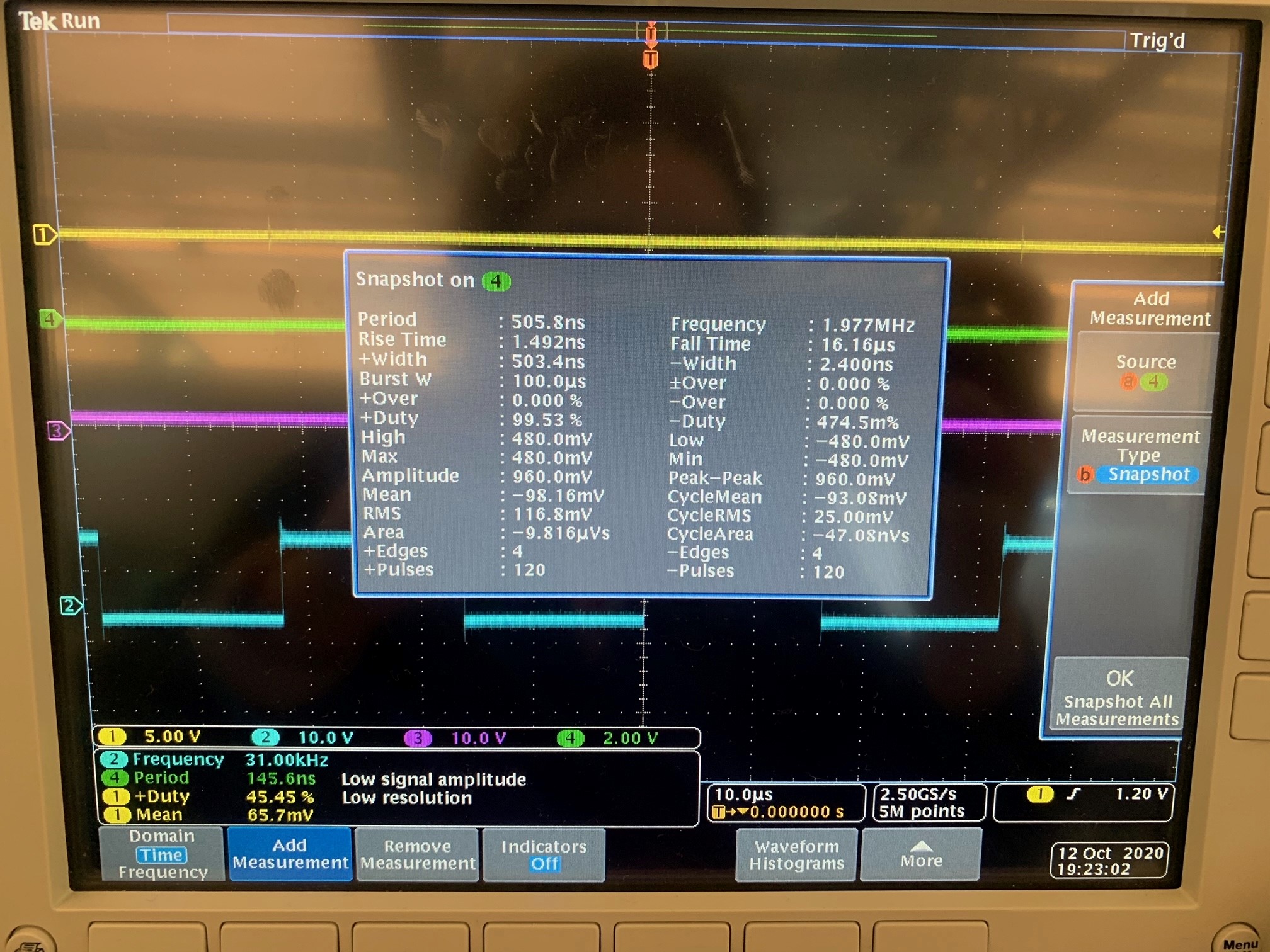
I am trying to write code on the EK-TM4C1294XL that will produce a PWM wave that controls the DRV8803 on the DRV8803EVM board.


What I want to do is use the EK-TM4C1294XL to turn on and off a solenoid using the DRV8803EVM board, according to the DRV8803 datasheets I need to have a PWM to trigger the motor drive function of the DRV8803. On the DRV8803EVM board, I don't want to use the microcontroller because I am applying external signals from the EK-TM4C1294XL. From my understanding of the DRV8803 timing diagram, I need to have a PWM that will stay high until the solenoid needs to be turned on and then the PWM will go low, am I correct in this thinking?


Based on my understanding I have written the code below. However, when I connect the EK-TM4C1294XL to the DRV8803EVM board (which I believe I have set up correctly according to the diagram) I don't get anything from the outputs of the board. I have pasted the code I am using below.

////*****************************************************************************
#include <stdbool.h>
#include <stdint.h>
#include "inc/hw_memmap.h"
#include "driverlib/gpio.h"
#include "driverlib/adc.h"
#include "driverlib/pin_map.h"
#include "driverlib/pwm.h"
#include "driverlib/sysctl.h"
#include "driverlib/uart.h"
#include "utils/uartstdio.h"
//////*****************************************************************************
//////
////// This function sets up UART0 to be used for a console to display information
////// as the example is running.
//////
void
GetADC(void)
{
#if defined(TARGET_IS_TM4C129_RA0) ||                                         \
    defined(TARGET_IS_TM4C129_RA1) ||                                         \
    defined(TARGET_IS_TM4C129_RA2)
    uint32_t ui32SysClock;
#endif

    uint32_t pui32ADC0Value[1];
#if defined(TARGET_IS_TM4C129_RA0) ||                                         \
    defined(TARGET_IS_TM4C129_RA1) ||                                         \
    defined(TARGET_IS_TM4C129_RA2)
    ui32SysClock = SysCtlClockFreqSet((SYSCTL_XTAL_25MHZ |
                                       SYSCTL_OSC_MAIN |
                                       SYSCTL_USE_PLL |
                                       SYSCTL_CFG_VCO_480), 20000000);
#else
    SysCtlClockSet(SYSCTL_SYSDIV_10 | SYSCTL_USE_PLL | SYSCTL_OSC_MAIN |
                   SYSCTL_XTAL_16MHZ);
#endif

UARTprintf("ADC ->\n");
 //  UARTprintf("  Type: Single Ended\n");
 //  UARTprintf("  Samples: One\n");
 //  UARTprintf("  Update Rate: 250ms\n");
   UARTprintf("  Input Pin: AIN0/PE3\n\n");

   //
   // The ADC0 peripheral must be enabled for use.
   //
   SysCtlPeripheralEnable(SYSCTL_PERIPH_ADC0);

   //
   // For this example ADC0 is used with AIN0 on port E7.
   // The actual port and pins used may be different on your part, consult
   // the data sheet for more information.  GPIO port E needs to be enabled
   // so these pins can be used.
   // TODO: change this to whichever GPIO port you are using.
   //
   SysCtlPeripheralEnable(SYSCTL_PERIPH_GPIOE);

   //
   // Select the analog ADC function for these pins.
   // Consult the data sheet to see which functions are allocated per pin.
   // TODO: change this to select the port/pin you are using.
   //
   GPIOPinTypeADC(GPIO_PORTE_BASE, GPIO_PIN_3);

   //
   // Enable sample sequence 3 with a processor signal trigger.  Sequence 3
   // will do a single sample when the processor sends a signal to start the
   // conversion.  Each ADC module has 4 programmable sequences, sequence 0
   // to sequence 3.  This example is arbitrarily using sequence 3.
   //
   ADCSequenceConfigure(ADC0_BASE, 3, ADC_TRIGGER_PROCESSOR, 0);

   //
   // Configure step 0 on sequence 3.  Sample channel 0 (ADC_CTL_CH0) in
   // single-ended mode (default) and configure the interrupt flag
   // (ADC_CTL_IE) to be set when the sample is done.  Tell the ADC logic
   // that this is the last conversion on sequence 3 (ADC_CTL_END).  Sequence
   // 3 has only one programmable step.  Sequence 1 and 2 have 4 steps, and
   // sequence 0 has 8 programmable steps.  Since we are only doing a single
   // conversion using sequence 3 we will only configure step 0.  For more
   // information on the ADC sequences and steps, reference the datasheet.
   //
   ADCSequenceStepConfigure(ADC0_BASE, 3, 0, ADC_CTL_CH0 | ADC_CTL_IE |
                            ADC_CTL_END);

   //
   // Since sample sequence 3 is now configured, it must be enabled.
   //
   ADCSequenceEnable(ADC0_BASE, 3);

   //
   // Clear the interrupt status flag.  This is done to make sure the
   // interrupt flag is cleared before we sample.
   //
   ADCIntClear(ADC0_BASE, 3);

   //
   // Sample AIN0 forever.  Display the value on the console.
   //
   int y;
   y=0;
   while(y<5)
   {
       //
       // Trigger the ADC conversion.
       //
       ADCProcessorTrigger(ADC0_BASE, 3);

       //
       // Wait for conversion to be completed.
       //
       while(!ADCIntStatus(ADC0_BASE, 3, false))
       {
       }

       //
       // Clear the ADC interrupt flag.
       //
       ADCIntClear(ADC0_BASE, 3);

       //
       // Read ADC Value.
       //
       ADCSequenceDataGet(ADC0_BASE, 3, pui32ADC0Value);

       //
       // Display the AIN0 (PE3) digital value on the console.
       //
       UARTprintf("AIN0 = %4d\r", pui32ADC0Value[0]);
       UARTprintf("\n");
       //
       // This function provides a means of generating a constant length
       // delay.  The function delay (in cycles) = 3 * parameter.  Delay
       // 250ms arbitrarily.
       //
#if defined(TARGET_IS_TM4C129_RA0) ||                                         \
   defined(TARGET_IS_TM4C129_RA1) ||                                         \
   defined(TARGET_IS_TM4C129_RA2)
       SysCtlDelay(ui32SysClock / 12);
#else
       SysCtlDelay(SysCtlClockGet() / 12);
#endif
       y++;
   }
}
//////*****************************************************************************
void
InitConsole(void)
{
////////    //
//////Enable GPIO port A which is used for UART0 pins.
////////    // TODO: change this to whichever GPIO port you are using.
////////    //
   SysCtlPeripheralEnable(SYSCTL_PERIPH_GPIOA);
////////
////////    //
////////    // Configure the pin muxing for UART0 functions on port A0 and A1.
////////    // This step is not necessary if your part does not support pin muxing.
////////    // TODO: change this to select the port/pin you are using.
////////    //
   GPIOPinConfigure(GPIO_PA0_U0RX);
   GPIOPinConfigure(GPIO_PA1_U0TX);
////////
////////    //
////////    // Enable UART0 so that we can configure the clock.
////////    //
  SysCtlPeripheralEnable(SYSCTL_PERIPH_UART0);
////////
////////    //
////////    // Use the internal 16MHz oscillator as the UART clock source.
////////    //
  UARTClockSourceSet(UART0_BASE, UART_CLOCK_PIOSC);
////////
////////    //
////////    // Select the alternate (UART) function for these pins.
////////    // TODO: change this to select the port/pin you are using.
////////    //
   GPIOPinTypeUART(GPIO_PORTA_BASE, GPIO_PIN_0 | GPIO_PIN_1);
////////
////////    //
////////    // Initialize the UART for console I/O.
////////    //
   UARTStdioConfig(0, 115200, 16000000);
}


//////*****************************************************************************
#if defined(TARGET_IS_TM4C129_RA0) ||                                         \
        defined(TARGET_IS_TM4C129_RA1) ||                                         \
    defined(TARGET_IS_TM4C129_RA2)
    uint32_t g_ui32SysClock;
#endif
//////////
////////    //
//////    // Set the clocking to run directly from the external crystal/oscillator.
//////    // TODO: The SYSCTL_XTAL_ value must be changed to match the value of the
//////    // crystal on your board.
//////    //
  #if defined(TARGET_IS_TM4C129_RA0) ||                                         \
      defined(TARGET_IS_TM4C129_RA1) ||                                         \
       defined(TARGET_IS_TM4C129_RA2)
       // g_ui32SysClock = SysCtlClockSet((SYSCTL_XTAL_25MHZ| SYSCTL_OSC_MAIN | SYSCTL_USE_OSC), 1200000);
#else
  SysCtlClockSet(SYSCTL_SYSDIV_1 | SYSCTL_USE_OSC | SYSCTL_OSC_MAIN |
                   SYSCTL_XTAL_16MHZ);
#endif
////

    uint32_t sysclock;
////
    void main()
    {
        float PWM_FREQ;
        float CPU_FREQ;
        float pwm_word;
        int t;
        int i;
        InitConsole();
     //   GetADC();
////
        PWM_FREQ = 64000; //31.250kHz
        CPU_FREQ = 1000000;
        pwm_word = (1/PWM_FREQ)*CPU_FREQ;
    sysclock = SysCtlClockFreqSet((SYSCTL_XTAL_16MHZ |
                                                         SYSCTL_OSC_MAIN |
                                                         SYSCTL_USE_PLL |
                                                         SYSCTL_CFG_VCO_480), CPU_FREQ);
  //  GPIOPinTypeGPIOOutput(GPIO_PORTF_BASE, RED_LED|BLUE_LED|GREEN_LED);
        i=0;
while(i<20)
{
        SysCtlPWMClockSet(SYSCTL_PWMDIV_1);//Set the clock speed
        SysCtlPeripheralEnable(SYSCTL_PERIPH_PWM0); //Enable the correct port
        SysCtlPeripheralEnable(SYSCTL_PERIPH_GPIOG);//Enable the GPIO port
        GPIOPinTypePWM(GPIO_PORTG_BASE, GPIO_PIN_1);//Define the pine
        GPIOPinConfigure(GPIO_PG1_M0PWM5); //Comfigure the pin based on the datasheet
        PWMGenConfigure(PWM0_BASE, PWM_GEN_2, PWM_GEN_MODE_DOWN | PWM_GEN_MODE_NO_SYNC);//Set the modes
       // UARTprintf("Gen config successful\n");
        PWMGenPeriodSet(PWM0_BASE, PWM_GEN_2, 300);
        PWMPulseWidthSet(PWM0_BASE, PWM_OUT_5,PWMGenPeriodGet(PWM0_BASE, PWM_GEN_2)/128);
        PWMOutputState(PWM0_BASE, PWM_OUT_5_BIT, true);
        PWMGenEnable(PWM0_BASE, PWM_GEN_2);
        UARTprintf("Running1\n");
      //  GPIOPinWrite(GPIO_PORTF_BASE, RED_LED|BLUE_LED|GREEN_LED, RED_LED);
     //   SysCtlDelay(20000000);
        i++;
        GetADC();
}
    t=0;
while(t<20)
{
      SysCtlPWMClockSet(SYSCTL_PWMDIV_1);
      SysCtlPeripheralEnable(SYSCTL_PERIPH_PWM0);
      SysCtlPeripheralEnable(SYSCTL_PERIPH_GPIOG);
       GPIOPinTypePWM(GPIO_PORTG_BASE, GPIO_PIN_2);
              GPIOPinConfigure(GPIO_PG0_M0PWM4);
              PWMGenConfigure(PWM0_BASE, PWM_GEN_2, PWM_GEN_MODE_UP_DOWN | PWM_GEN_MODE_DB_NO_SYNC);
              UARTprintf("Gen config successful\n");
              PWMGenPeriodSet(PWM0_BASE, PWM_GEN_2, pwm_word);
              PWMPulseWidthSet(PWM0_BASE, PWM_OUT_4, PWMGenPeriodGet(PWM0_BASE, PWM_GEN_2)/128);

              PWMOutputState(PWM0_BASE, PWM_OUT_4_BIT, true);
             PWMGenEnable(PWM0_BASE, PWM_GEN_2);
             UARTprintf("Running2\n");
         //    SysCtlDelay(20000000);
              t++;
              GetADC();
}
////

   }

Any help with this would be much appreciated. 

Thank you

  • Hi Rachel,

    Thank you for posting to the motor drives forum.

    I have a couple questions:

    1. did you remove the 0ohm resistors (R15-R18)? those should be removed when connecting an external micro-controller.
    2. If the answer to (1) is yes, is the EK-TM4C1294XL properly outputting the PWM signal? 
    3. If answer to (2) is yes, Is nENBL and RESET logic low? is the power supply (VM) on?

  • Hello Pablo, 

    Here are the answers to your questions:

    1. Yes I did remove the 0ohm resistors. 

    2. The EK-TM4C1294XL is outputting a PWM signal but I don't think its the correct PWM signal to trigger the DRV8803... or that is my assumption because there is no output. 

    3. I do have nENBL and RESET floating (which should be fine because they have a pull-down resistor. VM is also powered on.  

    Thank you, 

    Rachel 

  • Rachel,

    Thank you for the information.

    In regards to answer (2), what PWM frequency and duty cycle are you using for IN1, IN2, IN3, and IN4? 

  • Pablo, 

    The PWM frequency for IN1 and IN2 is set at the frequency of 31.25 kHz (as specified by the DRV8803 which I think is right?). For the duty cycle, I have the period defined, the pulse width set, and the output state-defined but I don't think I defined a duty cycle anywhere. 

    Thanks, 

    Rachel

  • Rachel,

    What is the ON time and OFF time for both IN1 and IN2? If the ON time of the PWM signal is too short, the FETs in the H-bridge may not be fully turning on.

  • Pablo, 

    Right now I have a delay after turning it on for about 200000 seconds. The code below is how I am generating my PWM wave. I am not quite sure how to accomplish the ON and OFF state that you are talking about. 

    while(i<20)
    {
            SysCtlPWMClockSet(SYSCTL_PWMDIV_1);//Set the clock speed
            SysCtlPeripheralEnable(SYSCTL_PERIPH_PWM0); //Enable the correct port
            SysCtlPeripheralEnable(SYSCTL_PERIPH_GPIOG);//Enable the GPIO port
            GPIOPinTypePWM(GPIO_PORTG_BASE, GPIO_PIN_1);//Define the pine
            GPIOPinConfigure(GPIO_PG1_M0PWM5); //Comfigure the pin based on the datasheet
            PWMGenConfigure(PWM0_BASE, PWM_GEN_2, PWM_GEN_MODE_DOWN | PWM_GEN_MODE_NO_SYNC);//Set the modes
           // UARTprintf("Gen config successful\n");
            PWMGenPeriodSet(PWM0_BASE, PWM_GEN_2, 300);
            PWMPulseWidthSet(PWM0_BASE, PWM_OUT_5,PWMGenPeriodGet(PWM0_BASE, PWM_GEN_2)/128);
            PWMOutputState(PWM0_BASE, PWM_OUT_5_BIT, true);
            PWMGenEnable(PWM0_BASE, PWM_GEN_2);
            UARTprintf("Running1\n");
          //  GPIOPinWrite(GPIO_PORTF_BASE, RED_LED|BLUE_LED|GREEN_LED, RED_LED);
         //   SysCtlDelay(20000000);
            i++;
            GetADC();
    }
        t=0;
    while(t<20)
    {
          SysCtlPWMClockSet(SYSCTL_PWMDIV_1);
          SysCtlPeripheralEnable(SYSCTL_PERIPH_PWM0);
          SysCtlPeripheralEnable(SYSCTL_PERIPH_GPIOG);
           GPIOPinTypePWM(GPIO_PORTG_BASE, GPIO_PIN_2);
                  GPIOPinConfigure(GPIO_PG0_M0PWM4);
                  PWMGenConfigure(PWM0_BASE, PWM_GEN_2, PWM_GEN_MODE_UP_DOWN | PWM_GEN_MODE_DB_NO_SYNC);
                  UARTprintf("Gen config successful\n");
                  PWMGenPeriodSet(PWM0_BASE, PWM_GEN_2, pwm_word);
                  PWMPulseWidthSet(PWM0_BASE, PWM_OUT_4, PWMGenPeriodGet(PWM0_BASE, PWM_GEN_2)/128);
    
                  PWMOutputState(PWM0_BASE, PWM_OUT_4_BIT, true);
                 PWMGenEnable(PWM0_BASE, PWM_GEN_2);
                 UARTprintf("Running2\n");
             //    SysCtlDelay(20000000);
                  t++;

    Thank you, 

    Rachel 

  • Hi Rachel,

    Can you probe an oscilloscope to IN1 and IN2 to see the signals on a scope. I think that will be the easiest way to verify the ON time of the signal.

  • Pablo, 

    I will be able to take an oscilloscope reading tomorrow. I will reply with the answer here. 

    Thank you for your patience. 

    Rachel

  • Hello Pablo, 

    I have attached the measurements from IN1 and IN2 from the oscilloscope

  • Hi Rachel,

    IN1 and IN2 signals are not 31.25kHz as you wrote in your code and don't appear to be proper PWM cycles. Did you take the measurements with the external u-controller connected to the DRV8803EVM?

    Overall, the signals don't look correct. Either the PWM signals from the external micro-controller are not correct, or the signals become distorted when connecting to the EVM. Can you run another quick test? Try measuring the PWM  output of IN1 and IN2 directly from the external microcontroller output without connecting to the EVM?

    Also, if you have a signal generator, can you apply a 31kHz (50% duty cycle) waveform at IN2 and tie IN1 to GND (0V). Then measure the voltage at the driver outputs. I want to figure out if it is the EVM or the external controller causing the problem.

  • Hi Pablo, 

    I did not take the measurements with the DRV8803EVM attached. The measurements taken here are purely the output of PG0 and PG1 from the  EK-TM4C1294XL without being applied to IN1 and IN2.

    I will try the second test where I use a signal generator and apply a 31kHz (50% duty cycle) waveform at IN2 and tie IN1 to GND (0V) and then measure the voltage at the output. 

    Thank you, 

    Rachel 

  • When I used a signal generator and apply a 31kHz (50% duty cycle) waveform at IN2 and tie IN1 to GND (0V) and then measure the voltage at OUT1 I read 0.043V. 

  • What about the voltage at OUT2?

  • The voltage at OUT2 is -0.088V.

  • Rachel,

    I should have asked this at the beginning but are you using the GUI? You need to use the GUI to enable the device as per the instructions in the user's manual (https://www.ti.com/lit/ug/slvu574b/slvu574b.pdf?ts=1602176169053&ref_url=https%253A%252F%252Fwww.ti.com%252Ftool%252FDRV8803EVM)

  • Pablo, 

    I was planning on just using the  EK-TM4C1294XL to control the DRV8803 on the EVAL board. Do I have to use the GUI to accomplish what I want?

    I do have an external power source to power the evaluation board, and I have the MCU power jumper removed. 

    Thank you, 

    Rachel 

  • Rachel,

    Please disregard my previous reply. Yes, you don't have to use the GUI if you are using external micro-controller to provide the necessary signals to the board. I was thinking about the DRV8804EVM which has a serial interface that requires the GUI.

    So far we know that even providing an external clean PWM signals to IN1 and IN2, the outputs are low. The next step is to figure out if the driver is actually powered and the outputs are enabled. Can you provide the voltage measurements for the following pins with no load connected at the outputs and IN1 and IN2 connected to external signal generator (IN2=31kHz @ 50%DC and IN1=0V). 

    • Vm
    • VCLAMP
    • nENBL
    • RESET
    • IN1 (oscilloscope)
    • IN2 (oscilloscope)
    • nFAULT
  • Pablo, 

    This is what I have when IN1 and IN2 connected to an external signal generator (IN2=31kHz @ 50%DC and IN1=0V). 

    • Vm = 23.99V
    • VCLAMP = 23.99V
    • nENBL= 0.005V
    • RESET = 0.003V
    • IN1 (oscilloscope) =0.001V
    • IN2 (oscilloscope) = 4.35V
    • nFAULT= 2.09V

    Thank you, 

    Rachel 

  • Hi Rachel,

    Sorry again but I have a few more questions.

    1. Did you measure the voltages using an oscilloscope and measuring the max voltage vales or using a voltage meter? the value of nFAULT=2.09V but it should be equal to around 3.3V. That doesn't make much sense unless nFAULT is toggling from high to low and you measured it with a voltage meter. Can you double check the nFAULT signal with an oscilloscope.
    2. What is the amplitude of the PWM signal for IN2?

  • Hi Pablo, 

    1. I used a voltage meter to take the measurements. I do not have access to an oscilloscope again until Monday but I can double-check nFAULT then.  Should I also be measuring the OUT1 and OUT2 on the oscilloscope?

    2. Based on the measurement the amplitude for the PWM signal for IN2 is 3V.

    Thank you, 

    Rachel

  • Hi Rachel,

    Yes, we should be measuring both OUTx signals on the scope. Please take scope shots for IN1, IN2, nFAULT, OUT1 and OUT2. This will give us a good picture of what could be causing the issue.

  • Pablo, 

    I will do this Monday and get back to you, thank you for your help.

    Rachel 

  • IN1 is the yellow. IN2 is the blue. 

    nFault is purple. 

    Out1 is green. 

    Out2 is yellow. 

  • Hi Rachel,

    Here are my comments on the scope images:

    1. IN2 max voltage is 9.4V which is greater than the recommended max voltage for INx pins. This could damage the IC. I would suggest trying to run the EVM with the GUI to test if the IC is damaged.

      the value of IN1=1.3V which is greater than 0.6V which is the typical logic low voltage value specified in the datasheet. Assuming that no damage occurred from the high IN2 voltage, both IN1 and IN2 will be registered as logic HIGH by the IC which will placed OUT1 and OUT2 in a low state. 
    1. Please retake the measurements but this time adjust the PWM signals until the min voltage is close to 0V and the maximum value to 3.3V

  • Hi Pablo, 

    1. I retook the measurements with the changes you suggested, here are the results below. 

    IN2

    OUT2

    2. I also did what you suggested and tried to use the GUI to test if the IC is damaged from the overvoltage. I have powered on the EVM board with an outside power source and I have also connected the EVM to my computer and I am using the GUI to I am reading IN1, IN2, OUT1, and OUT2. I have the jumper on for MCU power and no matter what I change on the GUI I am not getting any change on the scope, which to me means there are two causes of this. Either the IC is damaged, or I don't have the GUI and the EVM set up correctly. 

  • Hi Rachel,

    1. You should be seeing some toggling at OUT2. This make me think that the device was damaged. I will try to recreate your set-up in the lab using the DRV8803EVM to see if I get the same results as you. If I do get the same results, then we'll have to figure out what is causing the problem.
    2. Did you solder in the 0Ω resistors when connecting EVM to GUI? If you did not, then that would explain why IN1 and IN2 are not changing. Even if the driver IC is damaged, IN1 and IN2 should be changing if the GUI and EVM are properly connected. Did you follow the steps on the user's guide?

    Expect a reply from me by 10/16. Thanks in advance for your patience.

  • Pablo, 

    1. Thank you for trying the test set up I appreciate it. 

    2. I did forget to solder the resistors back on, I will solder them back on and try again. I did follow the steps on the user's guide, but it may be different with the resistors soldered on now. 

    Thank you, 

    Rachel Roberts 

  • Rachel,

    I did not get the chance to do the test with the EVM.

    Were you able to retake the scope images with the resistors soldered back in?

  • Pablo, 

    Yes, I was able to retake the scope images, they are below:

    IN1 is the Blue

    Out1 is the Yellow 

    Based on these images I think it's safe to assume that the IC is damaged.

    Let me know your thoughts. 

    Thank you, 

    Rachel 

  • Hi Rachel,

    I believe the device probably is damaged, I suggest buying a new IC and replacing with damaged IC or getting a new EVM board. Once you have a new IC, try retaking the data again.

    I will close this thread for now but feel free to reply if you have any questions. If the thread is locked, you can ask a related question.