This thread has been locked.

If you have a related question, please click the "Ask a related question" button in the top right corner. The newly created question will be automatically linked to this question.

DRV8353: Problem with gate charge / discharge

Part Number: DRV8353
Other Parts Discussed in Thread: TMS320F28069,

Hello,

I am working with a motor control custom board that includes a DRV8353 driver and a TMS320F28069 microcontroller. We are using instaspin library to control the PMSM motor.

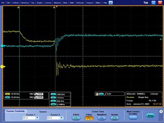
The board normally works ok, but sometimes the drive break specially when high Idrive values in the driver configuration are used. We have plot the voltage at the mosfet gates and we have seen something quite strange. The following picture shows the voltage at GHA pin (yellow) and GLA pin (blue). As you can seen the  voltage at GHA pin starts to decline from 34V (please, notice that signal are refered to GND), but it doesn't fall to 0V. When the Low side mosfet is triggered, the higw side gate volltage fall to 0V, but an oscillanting transitory signal is seen (negative voltage are also observed)

Figure 1: 

We have also seen that this transitions do not present the same pattern always. The following figure shows the same measurement, but in this case the voltage at GHA seems to be correctly performed

Figure 2

Figure 1 happens when DRV switches off the High side mosfet while one of the other high side mosfet is switched on.

Figure 2 happens when DRV switches off the high side mosfet and no other high side mosfet is switched on

We have tested with various Idrive configurations. With low Idrive values the spikes nearly dissapears, but the GHA voltage is not always drive to 0 before the low side is switched on (as in the first image). 

Do you have any advice?

Thank you in advance

  • Hi Borja, and thanks for your question!

    Our experts will get back to you tomorrow!

    Thanks,

    Matt

  • Hi Borja,

    Please note that it is OK to reference GLx to GND, however GHx should be referenced to SHx. This is because if you reference the high side gate to ground, you will be measuring the voltage drop at SHx + the High side gate.

    Reading the waveform left to right, we see that the high side MOSFET is turned on and is sitting at about 34V. Once the high side MOSFET is turned off, the voltage on the gate doesn’t drop to zero. Instead the voltage drops down to SHx, which is about 24V. This is because the current through an inductor can’t change instantaneously. Once the high side MOSFET is turned off, current flows from SHx up though the high-side MOSFET body diode into the supply. Once the low side MOSFET turns ON, then the current will stop flowing up through the high side body diode and start flowing through the low-side MOSFET. Now SHx is pulled to ground.

    Also, please see the link below, it covers selecting the best IDRIVE setting and why this is essential:

    https://e2e.ti.com/support/motor-drivers/f/motor-drivers-forum/796378/faq-selecting-the-best-idrive-setting-and-why-this-is-essential

    I hope you found this helpful.

    Thanks

    Michael

  • Hi Michael,

    I am Borja's co-worker.

    Thanks for your answer. It has been very helpful.

    We have selected a lower IDRIVE configuration (IdriveP = 150 mA / IdriveL = 300 mA) and we have experienced that the ringing signals that occurs when low side MOSFET turns ON have decreased. 

    However, we want to avoid negative peaks that could break the Driver. Looking in the forum, we found a thread named " DRV8353: Problems with newe Batch NR. TI98F and TI99F" (https://e2e.ti.com/support/motor-drivers/f/motor-drivers-forum/966354/drv8353-problems-with-newer-batch-nr-ti98f-ti99f), where this issue was discussed. The guy who opens the thread mentioned that they placed a fast reponse diode from GLx to GND to reduce the negative peaks. Your work mate Cole Macias close the thread due to this part of the response was covered over email. ¿Could we know what was the solution given by TI?

    I have tried to ask a related question from the thread, but the web page is not working properly.

    Thanks in advance.

  • Hi Gorka,

    In that thread the customer ended up opting for a RC snubber and the low side GS diode to fix their issue. However, I don’t know the number for the diode they used. In general, we recommend using both the diode and the capacitor.

    The diode will help but it isn’t the only recommended method for suppressing the ringing. All the diode does is it moves current around that is produced by the bouncing, and clamps the voltage so no absolute rating is violated.

    Now onto the capacitor. The capacitor actively sources (or stores) charge to even out voltage produced by the bouncing. Also, power losses are worse through a diode where it would be better to get rid of the ringing just through a capacitor.  10nF is fine for the HS drain to LS source cap though is subject to change. In the grand scheme of things, smaller caps are higher impedance for higher frequency. So you might have some low frequency ripple on these small caps but they attenuate that ripple.

    I've attached a FAQ that talks about proper RC snubber design for motor drives. You may find this helpful. 

    https://e2e.ti.com/support/motor-drivers/f/motor-drivers-forum/991693/faq-proper-rc-snubber-design-for-motor-drivers

    Thanks,

    Michael

  • Hi Michael,

    Thanks for the answer.

    I have one doubt. When you say "the low side GS diode to fix their issue", you mean The Gate and Source of the Low side Mosfet or between the pins GLx and SNx of the Driver? 

    In the previous threard, your work mate Cole mentioned the following: "Assuming the purpose of the diodes is to suppress transients on the gate during very high voltage events, I would recommend a)". In this case, a) was the chocie GLx and SNx (GND).

    Thanks in advance.

    Gorka

  • Hello Gorka,

    I've been helping Michael with this recommendation. The correct one is GLx and GND. I forgot to acknowledge that the SLx is usually attached to the top of a sense resistor which isn't always a stable node to supply current, especially since the shunt resistor will add inductance in the line which only adds to more ringing. An example is boxed below:

    Best,

    -Cole