This thread has been locked.
If you have a related question, please click the "Ask a related question" button in the top right corner. The newly created question will be automatically linked to this question.
Hi Sir,
may we learn from you and check this layout design?
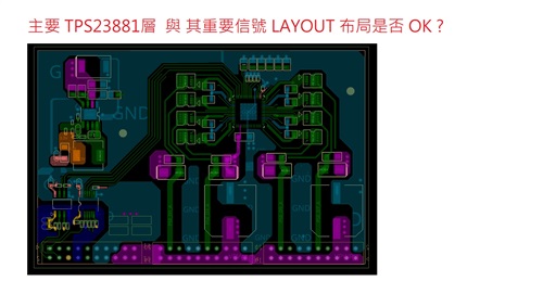
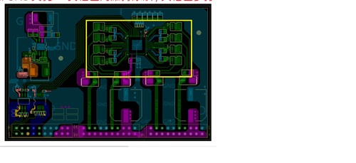
1. TPS23881 top layer and other important signal line.
2. except for the yellow area, other area use more the GND via hole, can it?
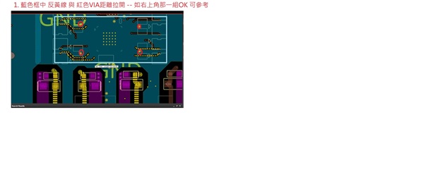
3. need to long the gap between red and yellow?
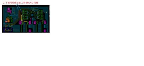
4. bottom layer.
Hi Tommy,
1. This layout looks okay
2. Yes more ground vias on planes near components that connect to ground will help create a short ground path to the IC.
3. Can you tell me what is the red traces?
4. If you can add ground stitching vias across the ground planes across the board this would be idea.
Can you also check 12.2.1 of the datasheet and make sure these components are correctly placed? Thanks!
Hi Sir,
thanks for your help and suggestion.
RESET/ INT/ OSS/SDAO&SDAI/ SCL pin.
Hi Tommy thanks for confirming, I see no issue with the red and yellow trace proximity. Thanks!