This thread has been locked.
If you have a related question, please click the "Ask a related question" button in the top right corner. The newly created question will be automatically linked to this question.
Hi Team,
i have a customer inquire about the followig:
1. Is there a LAYOUT GUIDE?
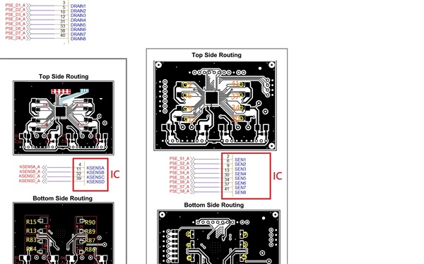
2. What are the requirements for the Via size indicated in the picture?
3. DRAIN1~8 follow the line to build the width. Can the surrounding signals be separated from the ground or must be cleared?
4. Are there special stacking conditions for 1.6mm board thickness/4-layer PCB?
Hi Tommy,
1) I would recommend looking at the layout considerations in the TPS23881 datasheets that look at the critical components. In general, the EVM would be a good reference as a known working layout soluiton.
2) The vias on the sense resistors are 40mil diameter with 18mil hole. I recommend using the same via size
3) In general we fill a large ground plane on both layers where possible to minimize noise injection on potentially sensitive traces. On the top layer it's not as easy to do close to the IC since there are pins on all sides of the IC.
4) We use two layers on the daughter card to optimize cost of the overall PSE system solution. However, if 4 layers is used, this will make the routing much easier. Typically, the power path traces will be on the top and bottom layers while the signal traces can be in the inner layers. Be sure there is a large ground plane on at least one of the layers.
Thanks!