


Hi team,
I'm working with my customer on the TPS53688 + CSD95410 project. And now they get some questions about the detection logic of the Pin-strap detection.
It sail in datasheet, I will short the upper resistor and then measure the low-side resistor. Could you let us know how the internal circuit work? We did some test with customer, waveform as follow.
The figure 1 up side / low side resistor are 43.2k / 20k. Figure 2 up side / low side resistor are 26.1k/20k. The time from rise up to lower side value detect is ~8msHowever, figure 1 show the detect waveform value get 60mV difference.
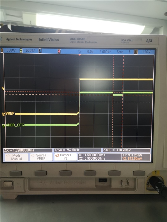
Figure 3 is another TPS53688 on another project, up side/ low side resistor are 1.2k / 20k. It's detect value is ~1.3V, and the time from rise up to lower side value detect is ~4ms
Since all the low side resistor is 20k, why there will be different value? And why the time from rise up to low side resistor value detect time is difference?
Could you help explain the internal working logic to help understand more abou the detect level difference and time difference?
Figure 1
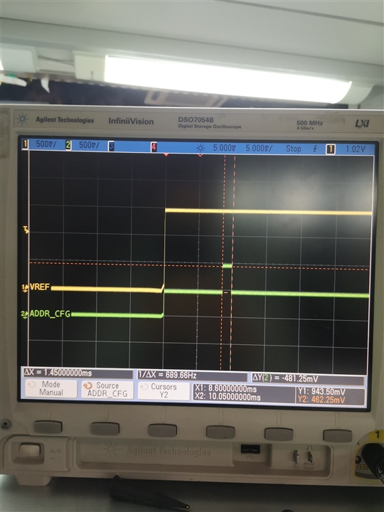
Figure 2
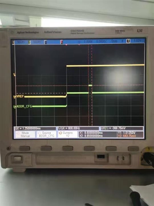
Figure 3
Best Regards,
Will
