This thread has been locked.

If you have a related question, please click the "Ask a related question" button in the top right corner. The newly created question will be automatically linked to this question.

TPS62733: Will this also work with a single 2032 coin cell alkaline? Powering C1101 Anaren Module

Part Number: TPS62733
Other Parts Discussed in Thread: TPS62730

The Docs always refer to 2 cell alkaline, not one. Can this work with a single?

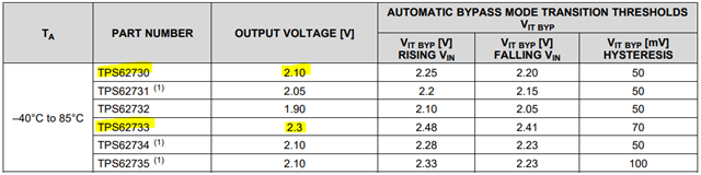
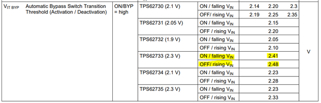
Also, the TPS62733 came recommended, however, at 2.1V, the ADC on my MPU430 requires 2.2V min which is higher than this output... is the 100mv difference a problem? (Not high accuracy ADC application, only relative change is needed).

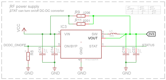
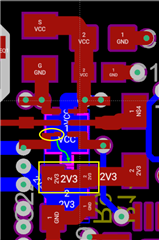
Meanwhile we did try the TPS62730 (2.3V output) and the output goes wild once battery starts to drop. The details on how this needs to be laid out are pretty lengthy. We'll get to that question later, assuming this will theoretically work.

Thanks or any tips!  Also, we have a bypass resistor (short) on the backside. Would this short trace from In/Out cause problems? I can cut them and try again... still learning. 

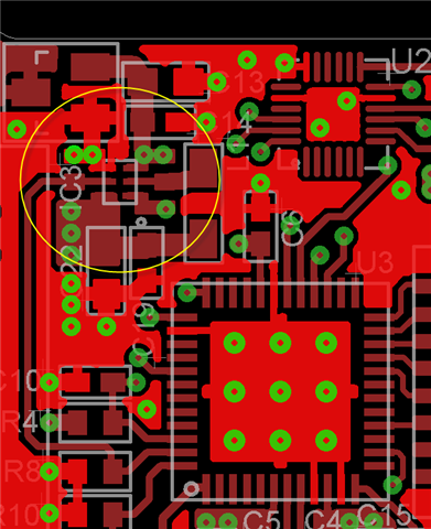
Can this be soldered? Wow it's small! My board supplier might have a problem here as well. (4PCB.com)

  • Hello John,

    Thanks for sending your queries to us.


    A single alkaline coin cell battery has a nominal voltage of 1.5V, which TPS6273x cannot support because its input voltage is limited to 1.9V minimum. If you use a lithium coin battery (ex. CR2032), TPS6274x can work it as the nominal battery voltage is 3.0V.

    TPS62730 has an output voltage of 2.10V and 2.3V for TPS62733 (see table below). So, it looks like you interchange the P/N's. Anyway, if your ADC needs a 2.2V minimum input voltage, then you should be using TPS62733.


    With regards to the Vout being erratic when the battery voltage is falling, try to remove the bypass resistor (R9 & R11). Please observed the output voltage if it becomes stable. 

    The device has an automatic bypass mode function (ON/BYP pin = High) which connects the battery to the output rail via a 2.1-ohm bypass switch. When the battery voltage (VIN) falls below the VIT BYP threshold, the internal bypass switch turns on and disables the DC-DC converter. Hence, an external bypass resistor is not needed.

    By the way, what is the effective capacitance of your output capacitors (C19/C22)? As highlighted in the datasheet, it should be in the range of 1.0uF to 10uF. In addition, it is difficult to check the schematic diagram. Can you share the PCB layout file? If it is confidential, then you send it via private message.

    Thank you.

    Best regards,

    Excel

  • We're going to try this chip again, so your input is very valuable now, thanks!!! 

    Here's the layout in Eagle. And yes I had the part #'s flipped, thx.

    C19/20 is 10uF + 2.2uF (too much actually). I might remove the one furthest away and trying lower the remaining one to 2-5uF range. The specs are pretty clear about keeping things tight and tidy. The inputs are also 10 and 2.2uF.

    R9/11 were only for elimination of the converter in case we ripped it out (and did temp). But just a theory, it has traces that go to the bottom side of the PCB and I was thinking this might be changing elect characteristics - just the traces and vias alone.  

    All components can go down to 2.1V (and I'll try both variants bc lower favors better battery life). But when that radio fires and other stuff comes on, my concern is the MPU will brownout. However, that fear may be unwarranted as it stems from how this layout below was running the MPU from the battery directly and using bypass for jtag updates. We don't need jtag anymore when our initial bootloader is preloaded. All works great, so this is like the last big hurdle. 

  • Hello John,

    Thanks for your quick feedback.

    First, there is no need to decrease the total nominal output capacitance (10uF + 2.2uF) because it should be within the maximum effective capacitance indicated in the datasheet (10uF).

    With regards to your PCB layout, one major concern is the connection of pin 6 (VOUT pin). It should be directly connected (and short as possible) to the output capacitors (C19/C22). How VOUT pin is connected to C19 & C22 because it is not visible? It would be best to follow exactly the reference layout shown in the datasheet (see page 19 of the datasheet).

    By the way, the main issue with your circuit is when the input voltage drop, the output voltage becomes unstable. Is it correct?  If that is the case, can you share a waveform with the following signals (VIN; VSW, VOUT pin, 2.3V/2.1V output)?

    Best regards,

    Excel  

  • Thanks again for the tips! 

    The old circuit wasn't all on 2.3V, was only for powering the radio. Maybe it will help to put whole board on 2.3v - in case there's a false bypass trigger in there somewhere. Terrified at trying even the smallest vibration motor on this load. That's like a 45 ma surge min. 

    I'll scope the next board, and start a new thread if needed. This one doesn't make a lot of sense to measure. So any last words are most welcome before I close. I think you spotted it really. 

  • FYI, Vout on Pin 6 is connect (after a ratsnest), but it's also fed to the backside which I'm thinking was a bad idea.


  • Hello John,

    Thanks for clarifying the PCB layout. Anyway, the VOUT pin should be connected to the output capacitor using a dedicated trace because it is sensitivity to noise. The output voltage can vary if a high amount of noise is injected to this node. I suggest the VOUT have separate trace going to the output capacitor as shown in the figure below. 

    Let me know if you have other concern.

    Best regards,

    Excel