


Other Parts Discussed in Thread: BQSTUDIO
Hi,This is the wave form across gate and source of discharge/charge FET,when enabled using FET_enable on bqstudio.The only difference between FET_enable and DSG_Toggle is that in FET_EN enables both CHG_FET and DSG_FET are turned on simultaneously.
Fig 2
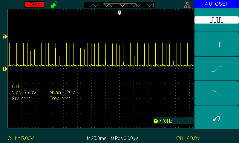
Fig 3
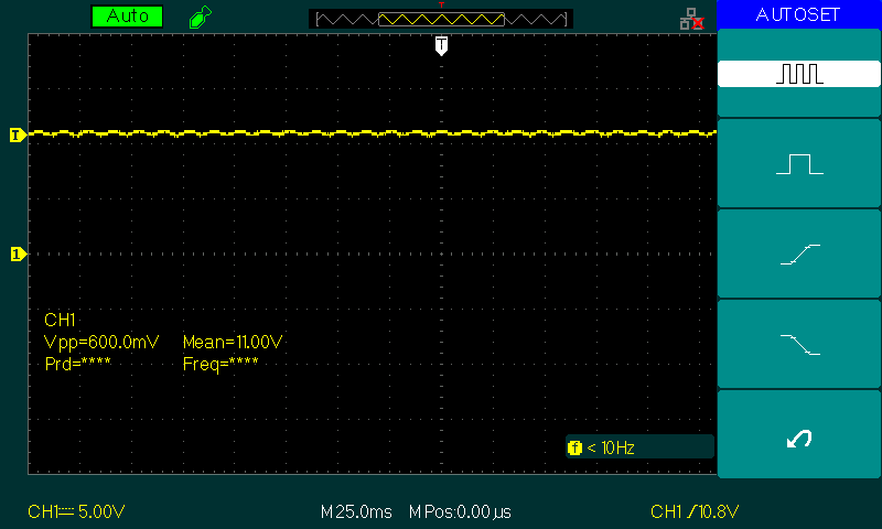
This is when DSG_Toggle was used.
What could be the reason for this behavior? Also I am not using Q1 and Q2 FETS so they are not connected.I am using only Q5 charge FET and Q6 discharge FET.
Initially turning on the CHG and DSG FET i e (Vgs=10.5V) and when load was turned on Vgs dropped to 0V. Later on replacing the FET the issue was fixed. I was able to discharge the pack at 15A for few minutes then I observed the oscillation similar to the fig2 and then the MOSFET turned off. Later on disconnecting the MOSFET from the driver ie(by removing R18,R20,R22,R23) and checking the CHG and DSG there was no output voltage although DSG_EN and CHG_EN were high.(I believe the driver is damaged). What is the reason for such oscillations and driver damage?
I am using 470nf capacitor for Cvddcp as per the table given in the data sheet. (The input capacitance of MOSFET is 13000pf ). A series gate resistor of 300E. Could this behavior occur if the Cvddcp is less or the series resistor is large. Or are there any other operation modes of the gate driver where the output is disabled.
