This thread has been locked.

If you have a related question, please click the "Ask a related question" button in the top right corner. The newly created question will be automatically linked to this question.

UCC21750: Oscillations in LTSpice simulation and adjusting soft turn off time without buffer

Part Number: UCC21750
Other Parts Discussed in Thread: UCC21732QDWEVM-025

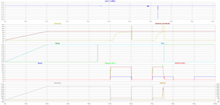
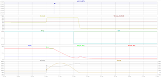
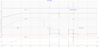
(1) I have been running a simulation in LTSpice evaluating the UCC21750 gate driver and require feedback with the waveforms I'm seeing. I'm seeing oscillations during turn-off and it would appear that there is some correlation with previous posts occurring the same fate of actual devices. We are in the process of purchasing the UCC21732QDWEVM-025 to evaluate this family of gate drivers to determine whether this is a suitable gate driver for our application.

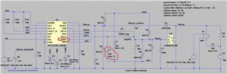
The simulation is as follows.
- 50kHz signal starting at 50us with 50% duty cycle.
- CREE C3M0016120D silicon carbide MOSFET used as the switching device (spice model provided by CREE).
- short circuit applied at 75us to test the soft turn off during a desaturation event.
- 700VDC bus voltage.
- resistive load of 10 Ohms.

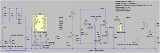
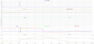
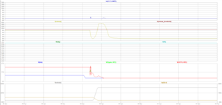
(2) The STO of the UCC21750 has an internal 400mA current source which is a little restrictive for our application. I have added an RC network to the simulation to vary the STO time which was recommended by TI when using a buffer circuit to enhance the current drive capability. The simulation appears to function correctly with the RC network however, I would like confirmation by TI that it's acceptable to use the UCC21750 in this fashion? It functions better when the active clamp circuitry is disabled. 

  • Hi Antonios,

    For 1:

    It is typical to see gate signal oscillations due to the switching transients although these oscillations can be mitigated in the application.

    1. Fine tuning of RG_OFF: Depending on the oscillations seen on the gate the external turn off resistor can be increased to minimize the magnitude of the oscillations. In the fine tuning there will be a trade off between acceptable gate oscillations and acceptable switching loses. Gate oscilations can also be mitigated with the following methods.
    2. Minimizing gate loop stray inductance: By placing the gate driver as close to the gate of the FET or IGBT will minimize the parasitic inductance that contributes to the magnitude of gate oscillations
    3. Adding additional components to the gate loop path: Additional components such as a ferrite bead and clamping diodes can also be implemented in the gate loop path. For prototype build it is recommended to have the foot print of these components to enable testing if necessary.

    For 2:

    The addition of the RC network is not typically implemented in design without a current buffer as having the capacitor in parallel with the gate will increase the witching losses in an application. Would you be able to share more details on your main concern with the 400mA soft turn feature of the UCC21750?

    Best regards,

    Andy Robles

  • Andy,
    Thank you for your prompt reply and the recommendations. Below are my responses to your comments.

    (1) Understanding we are likely to see oscillations in the application which can be mitigated by the points you have outlined, the simulation is more-or-less ideal. I expect these artefacts not to appear in the simulation. Simulating another gate driver IC with the same conditions I observe barely no oscillations. For example, the UCC21750 exhibits active clamping of about 15A soon after a desaturation event (as shown in the graph of my original post). Can you explain why the active clamping is activated?

    (2) We are currently evaluating the TI UCC21750 and the Infineon 1ED3491MC12M. The latter provides the ability to adjust the soft-off current source hence the question. What circuit do you recommend which gives the ability to adjust the soft turn off current without using a buffer circuit?

  • Hi Antonios,

    (1) I see the 15A spike you mention happens in the circuit where the CLMPI pin is not connected. This could be simply due to the importing of the model into LTSpice. Not having these pins properly connected could cause the model to output artifacts that don't correlate to the real gate driver behavior. Although our models work for the most part in the software LTSpice the model is only supported in TINA and PSPICE (Orcad/Allegro).

    I would recommend to move the simulation to TINA, which is similar to LTSpice, to get the most accurate representation of the gate driver since our models are supported in TINA.

    (2) There is no good way of adjusting the soft turn-off current of the UCC21750 without the external buffer circuit.

    • Do you have a previous design/version of this project in which a similar turn off current of 400mA showed concerns in the system around damaging the SiC FET or dissipating too much energy?
    • Is the main concern not having the flexibility to adjust the UCC21750 STO current as compared to the Infineon device?

    With your permission I can send you a friend request through this forum to share my contact info to take this to email so I can share some competitive analysis from our part based on the datasheets.


    Best regards,

    Andy Robles

  • Andy,

    (1) The 15A gate spike is with the CLMPI pin connected and the LTSpice simulation appears correct. I believe you mistakenly viewed the second schematic and not the first. Without the CLMPI pin connected, the current is no more than 3mA.

    (2) There is no previous design/version of this project in which a similar turn off current of 400mA showed concerns in the system around damaging the SiC FET or dissipating too much energy because this is a new project and as such, we're exploring new gate drivers.
    The main concern is not having the flexibility to adjust the UCC21750 STO current as compared to the Infineon device.

    I prefer if we didn't take this communication to email because I'd like other members of the community to benefit from this post. I've seen posts in the past which have moved to email that I would otherwise preferred to have stayed on the forum to assist in my decision. I would assume (and correct me if I'm wrong) you can share the competitive analysis from the part based on the datasheets very easily on this forum.

  • Hi Antonios,

    (1) Thank you for pointing that out. The internal miller clamp feature will only turn on when the voltage on the gate is measured to be VEE+2V(typ). Looking at the signals seems like at the time the short circuit was activated the 15A seen on CLMPI ocurred at the same time the VOUTH-VEE experienced a voltage dip that went lower than VEE. This does not look like typical behavior of gate driver signals during a short circuit the issues could be coming from using our modelin LTSpice, but we could also look into these signals further. Would you be able to zoom into this artifact into the simulation to more clearly see what is happening during the short circuit transient? With such a zoomed out capture it's hard to view the timing of the signals.

    (2) Looking into the datasheets I see a couple items I would like to comment on:

    • Isolation technology
    • Max working voltage
      • UCC21750 offers a higher max working isolation voltage(VIOWM/VIORM) which benefit comes from being able to operate the gate driver further from it's maximum voltage which is a safer zone translating to a longer lifetime
    • Shorter input to output propagation delay
      • Tighter propagation delay specs help improve system efficiency
    • Dedicated RDY and RST/EN pins
      • UCC21750 has a dedicated open drain output(RDY-pin) to report the status of the power supplies
      • UCC21750 has a dedicated RST/EN pin to shutdown the driver or reset the driver against any FLT conditions
    • Analog to PWM sensor
      • UCC21750 has an additional analog to PWM feature
        • An analog signal is feed into the AIN pin on the high voltage side and outputs a PWM signal, which duty cycle is proportional to the voltage on AIN, through the APWM pin
          • This feature can be used for temperature or DC bus voltage monitoring
    • Lower RθJA
      • Better thermal performance

    Let me know if there's any questions.

    Best regards,

    Andy Robles

  • Andy,
    Running the same simulation using the Infineon gate driver, large 15A clamping current spikes did not appear although I did witness 1.9A clamping currents during a turn-on event. As you pointed out, it may well be an issue with using your models in LTSpice.

    After changing the MOSFET from the original CREE C3M0016120D to an Infineon IMBG120R030M1H, the UCC21750 15A clamping current spikes were no longer present. The maximum clamping currents observed was 1.8A.

    I believe we have all the information we need to assess and compare the TI and Infineon gate drivers at the moment. I will post another message should the need arise.

    Thank you for your support.

  • Hi Antonios,

    No problem. Let me know if there's anything else I can do to help!

    Best regards,

    Andy Robles