Hello,
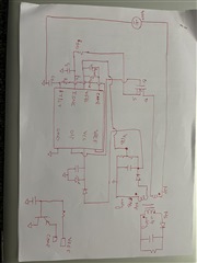
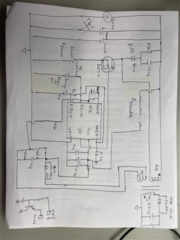
I am building an Emergency Power supply using flyback. My input voltage is 400V and output voltage is 12V. I am using peak current mode control. Can I use this configuration with auxilary winding for UC3842?

This thread has been locked.
If you have a related question, please click the "Ask a related question" button in the top right corner. The newly created question will be automatically linked to this question.
Hello,
I am building an Emergency Power supply using flyback. My input voltage is 400V and output voltage is 12V. I am using peak current mode control. Can I use this configuration with auxilary winding for UC3842?

Hi,
Yes, you can regulated the flyback from the aux winding the way you show in your diagram. Your schematic needs more work. Your current sense is not correct. Remove the current sense resistor as you have it shown, add a current sense resistor from the source of the MOSFET to GND, then place the current sense filter capacitor, Cc directly on the ISENSE pin by moving it to the other side of the current sense filter resistor, Rc. Between COMP and FB, you may want to add another capacitor in series the the Rcomp resistor. Add an RCD clamp across the primary transformer winding. Good luck with your design.
Regards,
Steve M
Hello,
I have connected the Rsense as suggested. For the capacitor in series with Rcomp, how to choose which value would work? Could I get any resources for this? Also, I am currently facing issues with the Vcomp. It is set at 1.3V and hence I don't see any significant Isns and output voltage. It would be helpful if I could get some suggestions for COMP pin as well.
Sincerely,
Aarohi

Aarohi,
The design looks much closer to at least having all the correct component placeholders. As far as designing the compensation, this will have some dependence on whether your flyback is operating in CCM or DCM and this will ultimately decide the value of primary magnetizing inductance needed which will determine your peak currents. I suggest you download and try TI Power Stage Designer. This is a very simple design simulation tool that is free from TI and runs local on your PC. You can select the topology, input your design parameters and see the waveforms over the all design corner cases. There is also a snubber design tool and compensation design tool you can try.
Steve M
Hello Steven,
Thank you so much. I designed my Type II compensation network with Rcomp= 200k, Ccomp= 500pF, Chf= 100pF. I tried giving Vcomp through a dc supply and varied it from 0.7V to 6V but still I get only 1.3V at the pin. I checked my closed loop compensation in matlab. My corner cases are: Vmin= 350V, Vmax= 400V, Rloadmin= 6.61 ohm, Rloadmax= 50 ohm. My phase margin is between 45,7 deg and 0 deg. I am designing a DCM flyback. As the power stage designer from TI supports only CCM, I could not use it. It would be really helpful if you could give some suggestions on how to debug the Vcomp. As Vcomp is stuck at 1.3V, after the following two diode drops, I get 0V and hence no significant ISNS.
Sincerely,
Aarohi
Aarohi,
From the Power Stage Designer front page, you select the flyback topology. You will see the screen below and you have to enable the "Discontinuous Conduction Mode" radio button, circled below. You can see that all four operating modes are supported
Click on any yellow highlighted component in the power stage and there are slider knobs you can adjust to view the ideal waveforms over your input/output parameter entered. Below are the waveforms for the primary MOSFET, Q1, and secondary side diode, D1.
As far as debugging your circuit, I can't help much with that but I suggest you break it down and simplify. Remove the start-up resistor and apply a fixed VCC bias from a DC lab supply so you can see how the VCC bootstrap winding is starting - or is it starting at all? Verify VREF=5V so you know the PWM is active. If the bootstrap winding is not coming up, this means you have no FB and therefore COMP is stuck low. Check the phasing of your transformer windings, verify the dot polarity, measure and verify the magnetizing inductance. Check the FB resistor divider network and make sure the resistor values are correct and soldered without any short or open condition.
One other comment: you should add a series gate resistor at the gate of your MOSFET ~10-30Ω and a parallel Schottky diode with the cathode pointing back toward the PWM OUT.
Regards,
Steve M
Typo: "no FB and therefore COMP is stuck low" should be "no FB and therefore COMP is high"