This thread has been locked.

If you have a related question, please click the "Ask a related question" button in the top right corner. The newly created question will be automatically linked to this question.

UC3845: QUERIES WORKING OF THE CIRCUIT

Part Number: UC3845
Other Parts Discussed in Thread: TL431

SMPS Circuit

Here I have attached a circuit which I have found in your datasheets for UC3845. I have taken same reference without any alteration. I have used UC3845 for this circuit. My desired output is of 15 V and 4 Amp. So I have changed only the value of Rfbu which is 12.51k and Rfbb which is 2.5k. According to datasheets I have used design formula which is mentioned for calculating these resistors value. But the thing is that when I run this circuit in hardware, there are no output voltages. Please suggests me how I can proceed. This is very urgent.

  • Transformer has been designed by taking reference of Texas Instruments

  • Champak,

    When you say "no output voltages" I assume you are referring to the 15V, converter output? What about the PWM controller? Start by measuring the pin voltages of the UC3845, especially VCC, VREF, OUT. Is VCC trying to start but then the bootstrap winding is not coming alive before UVLO_off is reached? How about a test where you remove Rstart and Dbias and apply an external lab supply directly to VCC so we can see the converter try to run without depending on startup. Break things down into smaller blocks and run each section as simple as possible. How about not using AC voltage at first and just apply DC input voltage only? Also, remove Cramp and replace with 0Ω jumper, Cramp is not needed and can cause problems with slope comp.

    If you have waveforms or specific questions during your debug, I'm here to help.

    Regards,

    Steve M

  • Hello Steven,

    Here "no output voltages" means I am referring to the 15V, converter output. One thing I will add that here I didn't connect Rss an Css. Please suggest me how I proceed? Please Suggest me test procedure step by step so that I can accomplish this SMPS circuit.

  • Champak,

    Not installing Css and Rss means you will not have soft-start but this has no impact on the converter not starting. Please follow the guidance I gave previous. To say "the power supply is not working, help me fix it", is not enough detail. I'm not in the lab seeing what you are seeing so you are going to have to debug your own design. I can help with specific questions about the operation of the PWM. The more specific you can be with your questions, the better I'm able to help. Waveforms, measured results, clear diagrams and targeted questions are always helpful.  Can you get the PWM to wake up using an external lab bias supply as I described previously? I would start there. Can you measure the magnetizing inductance of the transformer primary and is it what you expect for CCM or DCM operation as it is intended? Next I would verify the phasing  (dot polarity) of the flyback transformer, making sure it is constructed as you expect. The final thing to is to make sure you have a stable control loop that is meeting your design requirements and then go back and revisit the HV start-up so you can remove the VCC lab bias supply and get the converter to self bias.

    Regards,

    Steve M

  • Hello Stevan,

                       Firstly I would connect external supply to Vcc. So I am creating a 8.4 V dc supply and directly connecting to the Vcc.

    Is this voltage of Vcc sufficient to generate PWM for MOSFET? Please reply.CoreCoilformer2.pdf


    Transformer I have designed using this reference pdf which I have downloaded from Texas Instruments design portal. 

  • Hello Stevan,

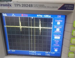
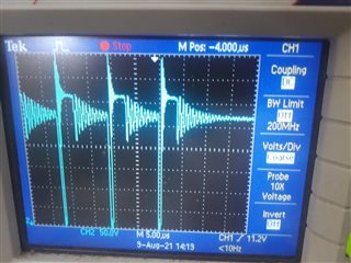
                       I have now tested this Circuit according to your suggestions. I have disconnected Rstart and Dbias. I have connected Vcc of UC3845 through external lab bias supply of 8.8V. I have connected 50 ohms resistor at the output terminal. Now I got output voltages of 14.1V. But my requirement is of 15V output. I am sharing waveforms in this reply which I got from test. Please suggests me what will be next steps which I will do.

    GATE TO SOURCE VOLTAGES

    The above waveform is of Gate to Source terminal.

    The above voltage is of Drain to Source Voltage waveform

    The above voltage is of Primary side voltage of Transformer

  • One more thing I am going to add, when I have connected 8 ohms resistor at output. The output voltage reduced to 7.8 volt. Please suggest how to stabilize.

  • One more thing I am going to add, when I have connected 8 ohms resistor at output. The output voltage reduced to 7.8 volt. Please suggest how to stabilize.

  • Champak,

    Congratulation, the converter is now switching. Next step is to snub/clamp the high frequency ringing seen at the rising edge of the drain-source waveform, stabilize the current loop then stabilize the voltage loop. Check your feedback divider, opto bias and COMP. For help, please download and try TI Power Stage Designer. This easy to use simulation tool runs local on your PC and includes a snubber design tool and control loop compensation tool you can experiment with.

    Steve M

  • Hello Stevan,

                        There are few questions which I am going to ask

    1. What will be the value of Rsnub and Csnub for snubber so that high frequency ringing will be minimized which has been seen at the rising edge of the drain-source waveform?

    2. How to stabilize current loop? I have chosen same component value as per given in slus223f datasheet. Which component I have to adjust to stabilize current loop?

    3. Which component I have to adjust to stabilize voltage loop?

    4.You have suggested to check feedback divider. I have chosen Rfbu as 12.51k and Rfbb as 2.5k by using formula which has been given in slus223f datasheet to get 15V output voltage. But the voltage get reduced at 9.5V when I am connecting 8ohms resistor at output as load. Why this is happening?

    5.What are the things I have to check for opto bias and COMP?

    Please reply. I am waiting for your valuable suggestions 

  • Hello Stevan,

                          Yesterday I have asked 5 questions and eagerly waiting for your reply. One more thing I am going to add that the voltage of VREF is 4.93 in my circuit. Is this correct?

  • Champak,

    1. What will be the value of Rsnub and Csnub for snubber so that high frequency ringing will be minimized which has been seen at the rising edge of the drain-source waveform?

    [SM]: Did you try using the snubber design tool in the TI Power Stage Designer I recommended? Most often the optimal RC values must be tuned on the the bench in the real circuit. You are trying to balance providing enough damping to tame the ringing to within an acceptable level for VDS and EMI vs power dissipation in the RCD clamp.

    2. How to stabilize current loop? I have chosen same component value as per given in slus223f datasheet. Which component I have to adjust to stabilize current loop?

    [SM]: The current loop can only be stabilized when the voltage loop is first stabilized. Add a dominant pole in the voltage error amp feedback and this will force the voltage loop stable. This is only temporary because your voltage loop regulation and small signal response will not be good but the goal is just to force stability so you can optimize the current sense signal. While holding the voltage loop stable, you can check the current sense signal at the PWM pin - make adjustments to the current sense resistor and RC filter as necessary to assure you have a smooth linear ramp. over the full line/load range of your design.

    3. Which component I have to adjust to stabilize voltage loop?

    [SM]: Voltage loop components set the DC gain, crossover freq, gain and phase margin of the control loop. Once the current sense signal from step 2 (above question) is known to be good, go back and remove the large cap you added to the voltage loop and now we can stabilize it. The components to adjust are Rcomp and Ccmop shown in your schematic. These are shown around the TL431 for the zero and the PWM pins1-2 for the pole.

    4.You have suggested to check feedback divider. I have chosen Rfbu as 12.51k and Rfbb as 2.5k by using formula which has been given in slus223f datasheet to get 15V output voltage. But the voltage get reduced at 9.5V when I am connecting 8ohms resistor at output as load. Why this is happening?

    [SM]: The feedback resistor values are correct for a 15-V output yet your regulation is not working. I suspect the feedback from the optocoupler is not correct and this is why I mentioned optocoupler bias needs to be checked. Measure the feedback pin voltage while the load is dynamically slowly changed. I bet your opto is current limited and giving all the feedback it can provide but the loop can't respond. It's like putting the gas pedal all the way to the floor and the car is at max speed but you need it to go faster than max. Try decreasing the opto LED resistor - use a trim pot and learn how the feedback works.

    5.What are the things I have to check for opto bias and COMP?

    Haver you tried running your design in Webench. I believe you are trying to design for universal AC input and Vout=15V, Iout=4A. The UC3845 Webench design and recommended component values are here. Between the Webench design and TI Power Stage Designer and the hardware you are testing, you should have all you need

    Steve M

  • Champak,

    Most of your questions are fundamental "how to" flyback power supply design questions that many others have already asked. There are a wealth of great app notes and design resources on flyback design, optocoupler/TL431 feedback circuits, current sensing etc.

    4.93 V measured at the VREF pin is low but within the specified range for UC3845. The blow range is given when VREF is sourcing less than 1mA max. Please be sure you are not overloading VREF:

    Steve M