A related question is a question created from another question. When the related question is created, it will be automatically linked to the original question.
If you have a related question, please click the "Ask a related question" button in the top right corner. The newly created question will be automatically linked to this question.
[FAQ] UCC27282: How to Correctly Size the Bootstrap Capacitor for Half-Bridge Gate Drivers
One of the most important gate driver design parameters is the selection of an adequate bootstrap capacitor. If the capacitance is too small, there will be insufficient charge available for the gate of the high-side transistor during switching. Consequently, this will lead to a diminished output voltage which may cause MOSFET heating, false logic, missing pulses, and lower efficiencies.
For practical applications the bootstrap capacitor should be 10x the minimum capacitance required to charge the gate of the high-side transistor each cycle. This makes the circuit more robust against nonidealities, such as capacitance shifts with temperature and voltage, transient and EMI events, skipped pulses, and allows the high-side transistor’s gate-to-source voltage to better track the supply voltage. Raising the bootstrap capacitance improves the margins of proper operation. However, there is an upper limit to the bootstrap capacitance set by the RC time constant of the bootstrap charging circuit and the minimum on time of the low-side transistor.
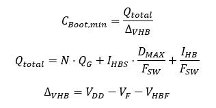
The theoretical minimum bootstrap capacitance can be calculated using the following equations:
Where N is the number of high-side transistors, QG is the gate charge of one transistor, IHBS is the max quiescent current from HB to VSS, DMAX is the max duty cycle, FSW is the switching frequency, IHB is the boot voltage quiescent current, VDD is the supply voltage of the device, VF is the bootstrap diode’s forward voltage, and VHBF is the minimum UVLO HB falling threshold with respect to HS.
Figure 1. Simulation Setup
Figure 1 shows the SIMPLIS schematic used to evaluate the performance of the UCC27211 half-bridge driver for varying bootstrap capacitance values. The device is operating at 250 kHz with a 50% high-side duty cycle. Figures 2 and 3 were obtained by varying the bootstrap capacitor C2.
Using the following datasheet values, a theoretical minimum capacitance for this circuit can be calculated: Qg=62.7nC, IHBS=1uA, D=0.5, Fsw=250kHz, Vdd=12V, Vf=0.65V, Vhbf=5.6V, IHB=100uA
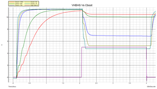
Figure 2. VHBHS for Varying Cboot Capacitances
Figure 2 shows the voltage across the bootstrap capacitor. Immediately at turn on, the bootstrap capacitor charges to the supply voltage, next, as the high-side output is enabled, the capacitor discharges to charge the high-side gate. Consequently, if this causes the bootstrap capacitor to lose a significant amount of its stored charge, the bootstrap voltage will fall.
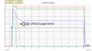
Figure 3. VHOHS for Varying Cboot Capacitances
Figure 3 shows the high-side transistor’s gate to source voltage. When the high-side output is switched on the high-side gate is charged, if this causes the bootstrap voltage to fall below the 5.6V UVLO of this driver, the high-side output is disabled and a logic error occurs.
Figures 2 and 3 illustrate that while it is possible to operate a driver with the minimum theoretical capacitance, it is not recommended. Additionally, it can be seen that when using a value close to the recommended 10x min value, the high-side output was able to maintain a higher more stable voltage.