A related question is a question created from another question. When the related question is created, it will be automatically linked to the original question.
If you have a related question, please click the "Ask a related question" button in the top right corner. The newly created question will be automatically linked to this question.
[FAQ] TPS62903: Reasons for Vout variations away from the expected value?
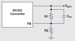
There are a couple factors that affect the output voltage accuracy in the TPS62x buck converters which include the selection of R1 and R2, regulation accuracy, and layout.
Selection of R1 and R2
One design challenge when selecting these resistors is the tradeoff of efficiency and feedback robustness.
The main benefit of having a high resistance for R1 + R2 is that it increases efficiency under light loads.
Otherwise the benefits of using lower resistor values include:
Reduced sensitivity to thermal, switching, and conducted noise
Better output voltage accuracy due to FB pin leakage current
Typically, the datasheet will list a maximum value for one or both of the resistors in the application notes section. For example, for the TPS6290x the recommended maximum for R2 is 400kΩ. However, in another case for the TPS6291x which is used in applications with low noise and low ripple, it is recommended to use an R2 less than 5kΩ. Acceptable values for R2 typically range from 1k’s to 100k’s Ohms depending on the end use case and design requirements like light load efficiency, output accuracy, and noise resilience. Once R2 is determined, R1 is selected using the voltage divider equation from Vout to Vfb.
Many of the newer mid-Vin (3-17V) low current (<6A) buck converters like the TPS62901/2/3 and TPS629210-Q1 also have a VSET option where the output voltage can be set using one external resistor from VFB to GND, taking advantage of an internal feedback network. For setting the resistive feedback networks, it is recommended to always use 1% resistors to obtain the best output voltage accuracy.
Regulation Accuracy
Another factor to consider if the output voltage is above or below the expected value is the feedback regulation accuracy of the device. Typically, the datasheet will list the accuracy of regulation on the feedback pin (FB) which may be listed as VFB in the datasheet. This can help explain why their may be a difference between the expected and measured values. It also may be useful to ensure that a minimum output voltage is not reached because of this tolerance by adjusting for it when selecting the feedback resistors R1 and R2.
Layout
Resistor value selection isn’t the only design choice in the resistive feedback network as the layout of this network is critical to ensure accurate voltage regulation. For the layout of the resistive feedback network it is a best practice to use a Kelvin connection as close to the output capacitor as possible in order to reduce the switching noise from the SW node and inductor. This is due to the high dv/dt nature of those traces that can introduce noise from capacitive coupling into the resistive feedback control loop. An additional layout tip when testing manufactured PCB boards is to ensure that all feedback connections are made properly and that there is no residual flux affecting the feedback resistors.