This thread has been locked.

If you have a related question, please click the "Ask a related question" button in the top right corner. The newly created question will be automatically linked to this question.

UCC28056: UCC28056 with GaNFET

Part Number: UCC28056

Hi,

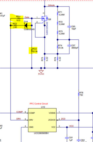
Could the UCC28056X DRV pin without charging and discharging circuit if used GaNFET? 

My customer used the NCP1623 for a new project PD100Wdesign, and the IC reference shows the gate pin without the dis/charging with GaNFET.

Thank you.

  • RG1, RG2 and D14 can be removed if the GaNFET has a built-in driver stage.  If not, then they would need to follow the FET manufacturer recommendations to safely and effectively drive the FET.

    RG3 (what the UCC28056 datasheet refers to as RDG) sets the minimum ZCD to DRV delay. The customer must consider the requirements of their system to determine the appropriate value to use for RGD.  If they are not sure of the final value of delay needed, I would recommend they put a placeholder resistor (DNI) in the design.

    See P7, P9 of the datasheet parameter value settings (RDGx, TZCDRx) and reference sec 8.3.3.1