This thread has been locked.

If you have a related question, please click the "Ask a related question" button in the top right corner. The newly created question will be automatically linked to this question.

BQ24272: In ready / charging status oscillation

Part Number: BQ24272
Other Parts Discussed in Thread: BQ24160,

Hi,

Some times the charger IC oscillates between "Charging" and "In ready". I have not been able to replicate the issue - the video is from the field.

The video displays all status registers. The voltage reading is for SYS pin.

I am wondering what can cause this to happen? The status registers do not show any faults. The battery voltage is about 3.7V - so not full at all. 

It seems like it is attempting to start charging, and then this is aborted.

When the battery has very low charge, the charger works - so this is anomaly occurs after a little while.

Having a detailed state diagram for when "In ready" is reported would be helpful in order to understand the stimuli which can cause "In ready" charger state to occur. 

The external power supply has also been replaced to rule out this as the culprit.

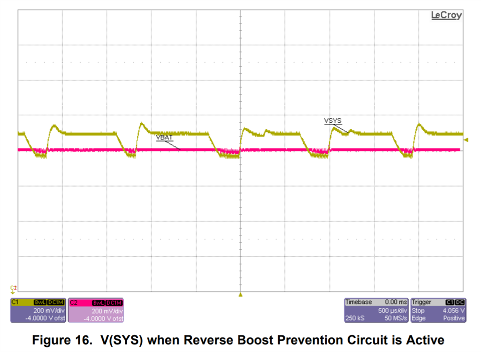
When "In ready" the SYS voltage is 4.295V and when "Charging" it is 4.166V. There is no AD pin connected to battery pin for battery voltage reading. This is read through SYS when power supply is not connected.

Any help is much appreciated. Thanks.

  • Hi Hans,

    IN Ready occurs when charge has stopped for reasons other than a fault (e.g. CE bit/pin disables charge, BAT or SYS OVP) or termination (Charge Done).  The charger also reports IN Ready while it is validating charge termination (termination deglitch time = 32ms + battery detection time = 250ms).  In this case, with V(SYS) = 4.295V and BATREG=4.2V (I assume), it appears that charge is complete or near complete but the charger is not terminating charge.  When this occurs, there will be a squarish waveform on SYS, similar to the plot below:

    If this squarish waveform is present, then the issue is related to the BQ24160 /27x family reverse boost prevention circuit, which disables termination, as explained on BQ24160 datasheet page 24. Reverse boost means the charger's buck converter is operating in unintended OTG mode with the buck converter working in reverse to provide a boosted voltage back at the input. The host can disable this prevention circuit in REG0x01b0.

    Regards,

    Jeff

  • Hello Jeff, 

    Thanks for your quick answer.

    My battery is about 5000 mAh 4.2V type cell. The termination current is set to 250 mA. Fast charge current is set to 925 mA. The BATREG is set to 4.16V in order not to fully charge the battery. This is to prolong the battery life.

    I agree with the various conditions which will report IN Ready, except for termination (CHARGE DONE). The STAT_2:0 can not report both IN Ready and CHARGE DONE at the same time - it must be either one. I agree that the internal state machine may be in In Ready state, but CHARGE DONE is still shown since this "other" state may take precedence in the I2C register perhaps.

    The battery voltage, for the case in the video, is about 3.7 to 3.8 V when under approximately 200 mA load (i.e charger plug is out). So I would conclude that charge is neither complete or near complete - far from it. Under normal conditions just after CHARGE DONE, when plug is out, we see the SYS voltage (i.e. Battery under 200 mA load) to be about 4.0 to 4.1 V.

    During testing in the lab, when the battery is under 200 mA load and the battery voltage is 3.8 V, then when charging immediately after I read 4.07V on the VBAT and the charge current is 0.80 A.

    There is already a dedicated button on the machine to turn off the prevention circuit (reverse boost detection circuitry). EN_NOBATOP is set to 1 when this button is pressed. When the button was pressed in the field, nothing happened. This may perhaps indicate that the anomaly is not related to the reverse boost prevention circuit?

    I made a new firmware patch in order to attempt to force the same anomaly in the lab. I made it possible to change the VBREG register by pressing up/down buttons - the VBREG value is also displayed on the display (incl. offset etc and multiplied with 20 mV). Unfortunately I was not able to replicate the issue.

    However, I found some interesting behavior: Given that CHARGE DONE is shown at VBREG 4.2V. If I then step the VBREG down it still reports CHARGE DONE until I reach a certain VBREG value of 3.96V where it now reports CHARGING. I can still turn it slightly more downwards and it still reports CHARGING. I measured the charge current (using a 10 mOhm series resistor in order to have a minimal burden voltage) and now there is actually current flowing out of the battery! Hence the battery is drained even though the IC is reporting charging! When I get to VBREG = 3.90 V the current drained from the battery is 140 mA. When I then set VBREG to 3.88 V, Battery OVP is reported as expected and 250 mA is drained from the battery - which is expected. I would expect that Battery OVP should be reported the moment current is drawn from the battery. What is the reason for this behavior?

    When the battery was drained I also measured VSYS on the scope, and the waveform was not as the one you showed me in the previous post - i.e. the conditions were not met (VBOVP > VBAT > VBATREG - VRCH).

    I can also verify that I see In Ready for a brief moment before Charge Done is reported when I step VBREG upwards.

    According to the datasheet for BQ24160 the reverse current protection is only active when VBOVP > VBAT > VBATREG - VRCH. The BQ24160 datasheet mentions that JEITA enabled ICs automatically lowers the voltage reference to 0.98 of the VBATREG value. The BQ24272 is specified as not JEITA compatible in the ordering information table, hence I do not scale with factor 0.98 for the below calculations.

    I tried to set VBATREG to various ranges between 3.9 and 4.2V, while reading the battery voltage. Example calculations below for VBATREG = 4.20 V. I was able to meet the condition, but only with small margin - hence I was unable to force the reverse protection circuit to turn on. How can I do this? Being able to replicate the issue (video) in the lab would be very helpful in order to find a workaround.

    • VBOVP = {1.025 x VBATREG , 1.075 x VBATREG} = {1.025 x 4.2 V , 1.075 x 4.2 V}  = {4.305 V , 4.515 V}
    • VRCH = 120 mV
    • {4.305 V , 4.515 V} > VBAT > 4.2 - 0.12 = 4.08 V.

    Regards HC

  • Hi Hans,

    Once CHARGE DONE is reached, the charger stays there until V(BAT) drops below VBATREG-VRCH or there is a SYS transient event that causes the charger to enter supplement mode where the battery must supplement the SYS load.

    Regarding This may perhaps indicate that the anomaly is not related to the reverse boost prevention circuit?, the only other instance of termination not occurring when V(BAT)>VBATREG-VRCH and IBAT<ITERM is if there is SYS transient that causes the charger to enter supplement mode for longer than the termination deglitch time (32ms) + battery detection time (256ms).

    Regarding What is the reason for this behavior?, if the charger is sinking battery current and the SW node has a pulse waveform while EN_NOBATOP=1, then the charger is reverse boosting (boost back).  There should be pulses back to input pin. 

    Regarding How can I do this?, adding series resistance >150mohm between BAT pin and battery or battery simulator with a low ITERM setting makes most charger ICs trip reverse boost prevention circuit.  In addition, if the battery is at a higher voltage than VBATREG so that  VBOVP > V(BAT) > VBATREG - VRCH, most devices trip reverse boost prevention circuit.

    Our recommended solution is to use a gauge or other ADC-like device to measure V(BAT) and I(BAT) perform termination instead of relying on the charger.

    Regards,

    Jeff