Other Parts Discussed in Thread: LM25118
user6144845
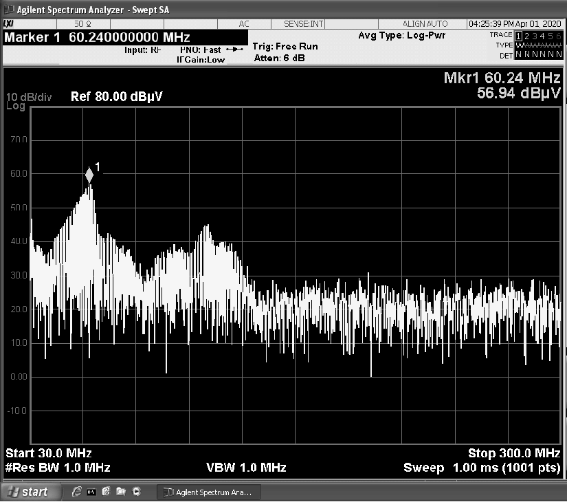
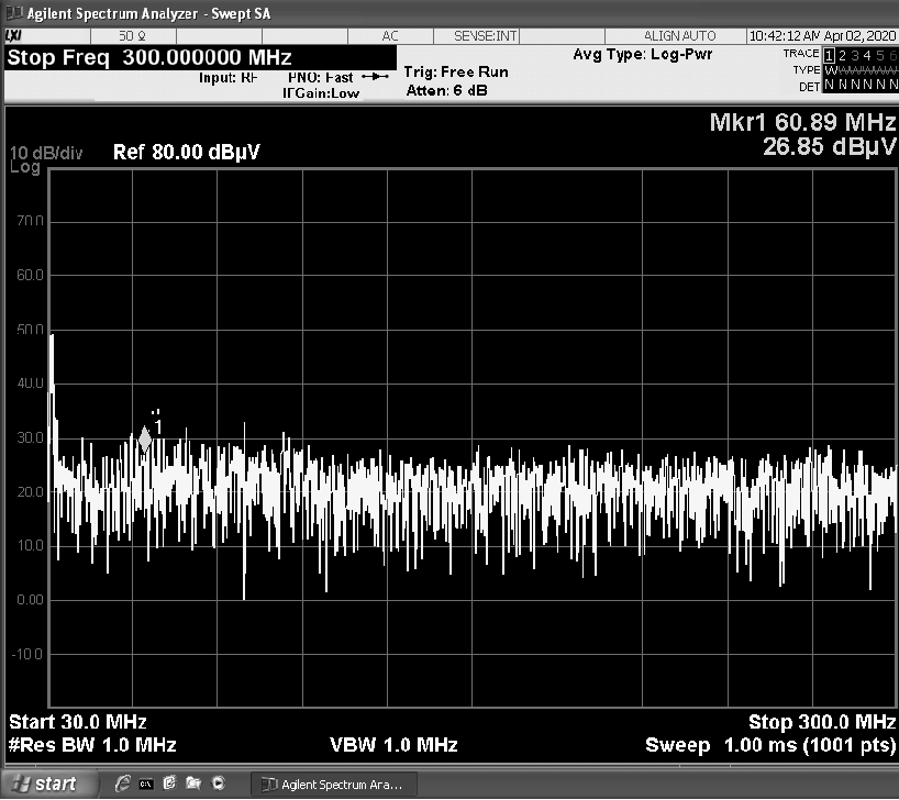
LM25118EVAL: Radiated noise of LM25118EVAL
This is a related question.
Hello.
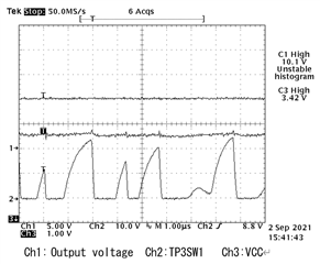
Although the noise due to the snubber could be reduced, the output voltage fluctuates when the input voltage is set to 30V or higher.
There is a voltage drop of VCC.
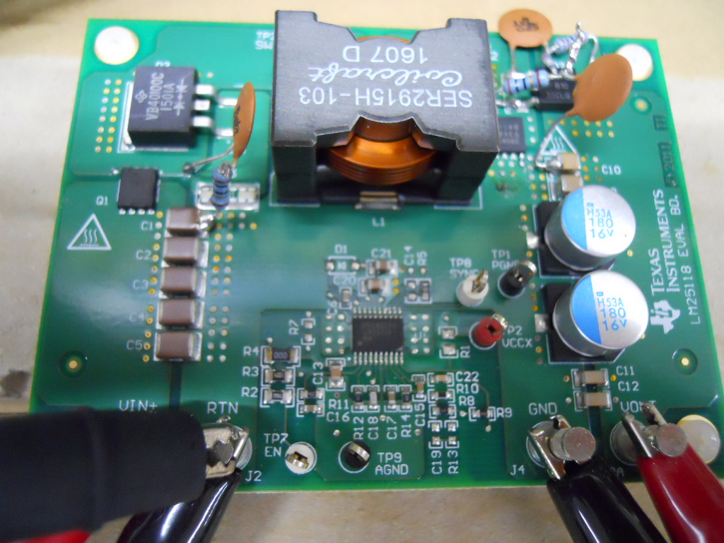
As I announced in the previous question, a snubber circuit (10Ω + 2000p) is inserted between GATE and SGND of Q1-Q2 of FET.
Please comment on the insertion location and constants.