This thread has been locked.

If you have a related question, please click the "Ask a related question" button in the top right corner. The newly created question will be automatically linked to this question.

UCC27712: Facing issue with top side Gate Pulse

Part Number: UCC27712

Hello,

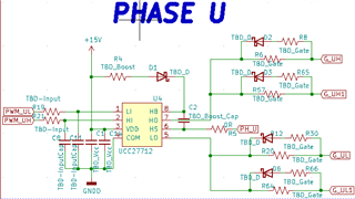
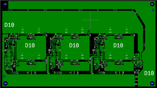
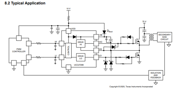
We are using UCC27712 for Our BLDC motor Driver,

but while testing we observer some strange Burst on high side MOSFET Gate pulse, due to which the output phase voltage is also behaving same

Requesting you to help on this

if You need more information regarding the Schematic and other thing, then that will share with you 

Thanks in advance

  • Hello Chaitanya,

    I believe this is the same schematic that you asked about here:

    https://e2e.ti.com/support/power-management-group/power-management/f/power-management-forum/1033341/ucc27712-gate-driver-selection-for-motor-driver-application

    I have some ideas but I am going to need some more information. 

    1. Can you provide a scope capture showing HO referenced to the HS node rather than ground? Either use a differential probe or use the scope's math function to subtract the switch node trace from the HO one you are showing. Can you also show LO simultaneously so we can see that the noise isn't caused by a slight shoot-through?
    2. Can you also get a capture of the bootstrap voltage (voltage from HB to HS)? This will help us tell if the issue is caused by the bootstrap circuit or not.
    3. Can you confirm if the schematic posted in the last thread is the same one we are working with here? What value of gate resistor are you currently using?
    4. Lastly, could you show the PCB layout of how the driver is connected to the FETs, as well as high-current paths? I believe you had a very high current system and that may be causing some ringing on the ground of the PCB.

    I look forward to hearing back from you.

    thanks,

    Alex Mazany

  • Hi Alexander,

    1)Will share you the Waveform by the End of the Day

    2)Will also share the Waveform

    3)The Schematic is attached below the Rg=10R (R6,R57,R20,R64) and other are 0R

    4) I've attached the Layout image

  • Thank you Chaitanya,

    I do not see any issues in particular with the layout or schematic. It is hard to make out the details of the layout, but it looks like the power planes are a good size. Good luck with capturing the waveform. Also, have you seen any damage to FETs or devices due to this pulse?

  • Hi Alexander,

    thanks for all your support

    I'm attaching the Gerber File So you can take a look of it

    also attaching the Waveform which we have captured while testing

    and last, there is no damage to any component until now. 

    UCC27712 Inverter Board Testing.docxUCC27712_InverterBoard.rar

  • Hello Chaitanya,

    Thank you for providing these captures. It seems that the driver has no issues with no load, which suggests that the issue is somehow coming from the motor. Most likely, the switching of the motor is causing inductive noise to appear on the switch node HS. This noise causes fluctuations on HB since it is referenced to HS, which then shows up on HO. I see you have a 0-ohm snubber resistor/jumper populated on HS; have you tried populating a resistor in this spot (maybe start with 5-10 ohms)? It should help reduce any noise on HS, but will slightly slow the bootstrap charging. Also, a Schottky diode from GND to HS very close to the driver can reduce the noise also, but would likely require a redesign. 

    As a side note, would it be possible to add in a small amount of dead-time with your controller? I'm not sure it will help, but it may be worth trying to see if it helps at all. 

    thanks,

    Alex Mazany

  • Hi Alexander,

      I've tried with 2.2R resistor get little improvement will do with 5 to 10R and check the result of the same

    The waveform which I've shared has a dead time of 1us,the dead time change is possible in controller.

    what amount of dead time would you recommend me to try?

    what you recommend us to avoid this noise in our new design (revision)

  • Hello Chaitanya,

    Can you get a measurement of just HS-GND on your scope to confirm it is appearing on the switch node? You could measure before and after the snubber resistor to see if it is helping at all as well. I just want to be absolutely sure this is the cause of the problem before you do any redesign.

    This diagram is for a different part, but the same ideas apply. The Schottky diode from GND to HS will conduct if a negative voltage appears on HS, pulling it to ground. This should help reduce the negative spikes on HS. It should be placed extremely close to the driver to maximize effectiveness.

    Regarding the dead-time, 1us seems to be working fine. However, your FETs have a pretty long rise/fall time of about 400-500ns, which is eating into the dead-time. It won't be good for the efficiency, but you could try something like 5-10us. Just as an experiment to see if it will help the system at all. I don't think this is the cause of your issue, but it would be nice to rule it out.

    Best of luck,

    Alex Mazany

  • Hi Alex,

    We have observed & captured the Waveform At all nodes of Gate Driver Including HS, We tried with different method and technique to minimize the Noise, but it still there,

    One More thing we've captured the Waveform of HO(High Side MOSFET Gate) and Inverter Ground Below the Low Side MOSFET after Shunt(the  Probe ground is connected Near to Supply Return,(The length is short))

    Please check the Below Waveform.

    Yellow-HO

    Blue- Inverter Ground

  • Hello Chaitanya, 

    This is a good observation; it looks like the ground noise is responsible for the issues in the pulses. Have you tried probing HIN and LIN? Those signals are referenced to ground so they may be seeing this noise, which could be causing the strange behavior on the outputs. Do you have a separate power and signal ground in your PCB? 

  • Hi Alex,

     We also captured the HIN and LIN they seeing the same noise which is replicating on output HO,the ground is separate but they are connected at supply return point i.e( - terminal).

    We want your valuable suggestions to suppress this noise issue and avoid it in our next revision.What might be the possible reason in our existing layout which is causing this kind of noise on Ground.(so we avoid that kind of mistakes)

    if you want a complete Schematic & Gerber to take a look of our system,that we can share with you.

  • Hello Chaitanya,

    I work with Alex and can help cover this device. If you can provide a schematic that shows the driver sections and the power Mosfet devices and any gate drive network, that will be helpful.

    If you are seeing noise on the driver input signals, from ground bounce or trace coupling, this can false trigger the driver and result in driver output unexpected behavior. I see you have R/C on the schematic for the LI and HI inputs but do not see the values. Confirm that the capacitors are close to the IC and connected to LI/HI and COM with short traces. It is better if the resistor is close to the IC as well. Try increasing the R/C values, starting with making C at least 100pF if there is high noise. 


    Regards, 

  • Hello Richarad,

    Thanks For Your Valuable Time,

    Please find the Attached Schematic & Gerber File of the Inverter Board

    HI & LI 47R & C is 33pF

    The capacitor & Resistor are placed close to the IC,

    5008.TI.rar

  • Hello again Chaitanya, 

    Looking at your zoomed in capture, it appears the major frequency of your noise is about 200kHz. Your RC filter will provide a cutoff frequency of about 500MHz, so a lot of the noise will easily get through. I would try upping the capacitance on the RC filter by a lot, possibly even up to 100nF. That may start to mess with your input signals, so keep an eye on them to make sure the RC filter doesn't distort them. In addition, you may be able to decouple the GND and PGND more. I don't know how exactly you have the power supplies setup for your board, but are you using the same ground connection for both your PGND and regular ground? Do you have any way to avoid that?

    thanks,

    Alex Mazany

  • Hi Alex,

    Yes we are using the Same ground for Both, Yes we have one 0R resistor Between The PGAND & GND (Gate Driver Signal ) by removing it we can avoid that.

  • Hi Chaitanya, 

    If you can reduce the noise by separating grounds rather than increasing your RC filter, that would be best. Please let me know if that works for reducing the noise on the inputs, and hopefully the outputs as well. 

    Good luck,

    Alex Mazany