This thread has been locked.

If you have a related question, please click the "Ask a related question" button in the top right corner. The newly created question will be automatically linked to this question.

TPS65261: Enable pin start delay using cap - discharge when off?

Part Number: TPS65261
Other Parts Discussed in Thread: AM5716

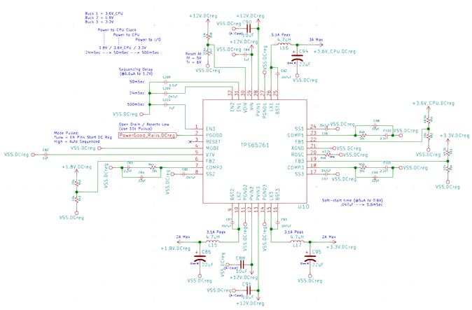
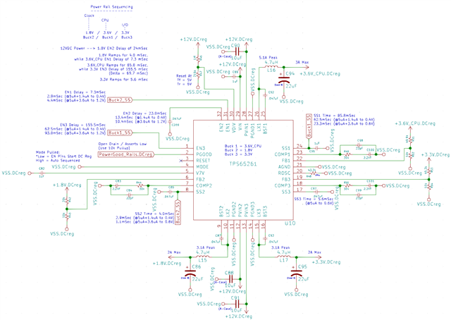
I am using the enable pins to sequence the startup of the three supplies for my application using an external capacitor charged from the internal current source.  It works perfectly to delay each supply, however I have noticed that the capacitors remain charged for quite a long time after removing power.  The result is that the supplies are not properly sequenced after a recent power off.  Is there a suggested circuit or method to discharge these caps reasonably quickly after power off?

Thank-you!
-Jason

  • Hi Jason,

    Could you try to add a bleeding resistor parallel with that capacitor?

    Thanks,

    Nancy

  • Hi, Jason 

    Could you send us the schematic? what is the value of ENx capacitors you used? 

  • I could, as a simple workaround.  I still worry a bit about a very quick power cycle where they have not bled down enough.
    I admit I haven't worked out an ideal combination of timings / component values.

  • Schematic is attached (as image).  Values are .047uF, 0.1uF, and 1uF

  • Hi, Jason 

    As Nancy said, paralleling bleeding resistor with Cen is one of workaround. 

    I am considering other workarounds, some questions: 

    It looks the power sequence: Buck2 --> Buck1 --> Buck3, right? 

    Is there any delay spec between Buck2 and Buck1, Buck1 and Buck3? 

    Do you have any requirement on power off? 

  • Hi Zhao,

    I appreciate you looking into it.  The spec for timing is based on powering a Sitara AM5716.  Buck 2 is the clock, Buck 1 powers the TPS659162 PMIC, and Buck 3 is I/O power.  I think there is quite a bit of wiggle room in the timing I set as long as the bucks come up in that order, and the PMIC (buck 1) has a chance to sequence (> 8mSec) before powering the I/O (buck 3).

    A simple resistor may be okay, but I'm not sure how much variation there is in the internal current sources (to rely on them if the majority of the current is going through the resistor to minimize bleed time), or if they can be driven constantly.


    -Jason

  • Hi, Jason 

    It looks you have spec on delay time between Buck1 and Buck3, > 8mSec, right? 

    Usually, the internal current sources have +/50% tolerance. 

    I suggested another workaround: 

    1. First, no need adding capacitors for EN1/3 pins. 

    2. Buck2 is fist come up, so keep 47nF for EN2 pin. 

    Connect SS2 to EN1 pin, and connect SS1 to EN3 pin. 

    3. In order to assure  > 8mSec delay, you can enlarge SS1 cap C96 > 33nS, so you can keep C96=47nF. 

  • Hi Zhao,

    I think I understand, and I like that this actually decreases the component count!

    I see that tying the SS pin to the next EN pin will sequence the next buck (with delay after getting up to voltage, since the pins have different thresholds).  One question I have is what happens after a quick power cycle - does the SS pin bleed down?  Hopefully it does, otherwise this would be another issue to solve, since there would be no soft start, either!

    Also, to clarify:
    -  In your workaround, I would keep all three 47nF SSx pin capacitors, correct?
    -  When tying the SS together with the EN, I assume both internal current sources would be additive?

    Thank-you for your continued assistance.  Much appreciated!

    -Jason

  • Hi, Jason 

    1. Yes, once BUCKx is disabled(ENx below threshold), the SSx will be discharged to 0V. 

    2. Yes, keep all of SSx cap (47nF).  

    3. Yes, the SSx and ENx source current will be additive. 

  • Okay, thank-you for your help!  I'll do as you suggested.

  • An updated schematic is below.  I increased the SS1/EN3 cap to 1uF; when tied together, the difference in the SS threshold and the EN threshold leads to the delay between buck1 being fully ramped up, and buck3 being enabled.  This should give me a ~69.7mSec delay (with plenty of room for 50% tolerance on the internal current sources.)  Hopefully I got this right.  Thanks again for your help!

    -Jason

  • Hi, Jason 

    The schematic looks good. 

    But there is one thing need to notice: 

    When IC is disabled, the SSx pin has about ~2kohm discharge resistor, with Css=1uF, the discharging time is about 3*RC constant = ~6mS, which means when doing power cycle test, the disable time must be larger than 6mS, otherwise, the 2nd startup will be the hard startup because SSx cap is not fully discharged.   

    Besides, suggest doing some verification on your board for this solution.