Other Parts Discussed in Thread: TPS22919, TPS61099, TPS61094
Hello, I upgraded low energy board layout with TPS61023 and TPS610994 converters. Could you check please? Screenshots:
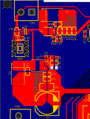
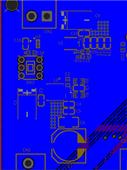
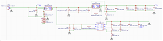
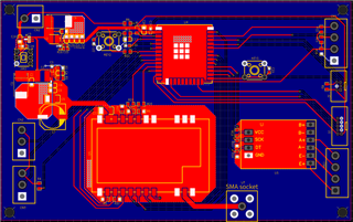
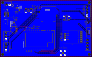
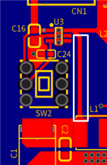
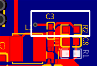
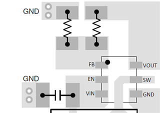
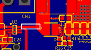
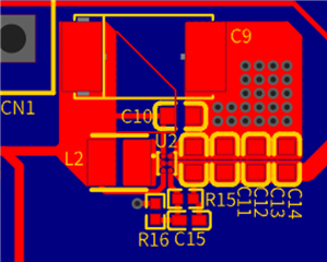
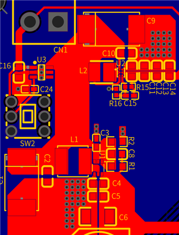
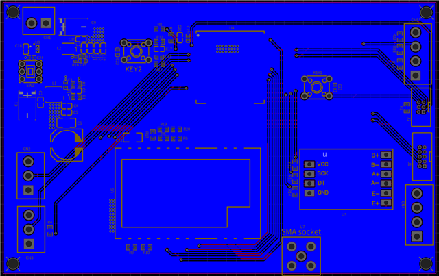
2 first screens are converters area, 3rd is converter and load switch schematic. 4 and 5 has GND highlighted. I got few questions:
1) Layout for TPS61023, TPS610994 (R15 and R16 will be used while it is TPS61099) and TPS22919 need any upgrades/changes (3V battery input at CN1)?
2) At pcb will be MCU (U4), radio module (U6), scale module (U5), one external i2c device on CN5 and 2 external analog devices on CN2 and CN3. Do I need do changes with grounding of my devices? GND will be whole bottom layer excluding tracks. (will it work stable with that GND, or need changes)
3) Should I make hardware changes with MCU GPIOs to reach as low as possible power consumption on GPIOs while not used (if yes, what chanes?), or it is just about software? (it will be mostly in sleep mode with very low power consumption but I am afraid of leaks at GPIOs)
Looking forward to hearing from you!