This thread has been locked.

If you have a related question, please click the "Ask a related question" button in the top right corner. The newly created question will be automatically linked to this question.

ISO5452-Q1: Input gate pulse getting disrupted at Pin 10 (IN+) of ISO5452QDWQ1 Driver IC

Part Number: ISO5452-Q1
Other Parts Discussed in Thread: ISO5452

Hi Ti,

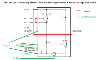
I am performing short circuit type -1 test based on AQG324 standard. I am using an external wire to short the High side switch and using a function generator to give gate pulse to the bottom side switch.

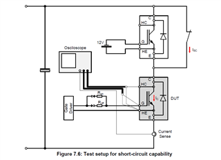
I am using ASPM16 Power module from Onsemi with the following modification 

I am using ISO5452 gate driver IC from TI for providing the gate pulse to the bottom switch. The gate driver design used is similar to unipolar output supply suggested in datasheet under chapter 10.2.2.1. For this test i am using isolated power supplies for VCC2. 

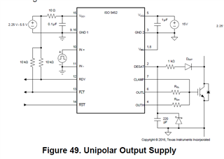
The RGH value is 8.25 ohm and RGL is 1.55 ohm.

A Signal is provided from Function generator to low side gate driver Pin 10 (IN+) of ISO5452QDWQ1 Driver IC, which is getting disrupted while performing the short circuit test at a bus voltage of 40v and higher, due which there is a false turn on & Turn off of power module.

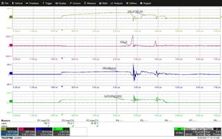
In the above Image, Green waveform is the Non-inverting gate drive voltage control input. Blue waveform is the Positive gate drive voltage output. Yellow waveform is gate emitter voltage (after gate resistor) at the IGBT gate pin. Red waveform is the collector emitter voltage of the IGBT. 

Request you to provide suggestions to mitigate this issue. 

  • Robin, 

    We already have an email thread going on this issue with our field team. I actually recognized this scope capture since we were discussing it internally last week. 

    Would you prefer to work on this here or stick to email? I can give some initial thoughts here, and let me know how you would prefer to proceed!

    First, I had some questions:

    Q: Is IN+ intended to be driven low at 3us, or 5us? 

    It nearly looks like a normal falling slew at ~3us, but if that were the case, I am not sure why IN+ would recover and hold high until 5us before going low again.

    Q: Are you testing this with TI's EVM, or using an internal board. If you could share schematic or even layout it would be helpful to see what is going on. 

    Q: Is there false turn-on when NO probes are connected? If not, please test and let me know. Particularly on the secondary side, the probes will couple a ton of noise when used with ground strap, ESPECIALLY in this kind of test. Probe and tip method (pigtail), or MMCX method are best for secondary side testing when possible. 

    Q: For this test, are Primary/secondary grounds (GND1/2) tied together? Isolated probe would be required otherwise if grounds remain isolated. 

    In email, I also saw you did have RC lowpass on your PWM input on IN-. Could you confirm whether this is populated for this test? If it is populated, could you share the position/layout for those components? if R/C are not close to the device pin this can contribute to this issue. 

    I also have a suspicion that the probing is causing a lot of the noise. For VGE / IN- waveforms, the noise magnitude is so large it would actually damage the driver. 

    Take for example the difference in VGE_before_RG and VGE_after_RG (closest to gate). The "before RG" signal should actually show less ringing due to the effect of RG, but we actually see significantly more noise than in the "after RG signal", which makes me think there is a difference in probing between those two signals. VGE after rg actually looks pretty clean. Are you probing those two signals differently? Photo or diagram of probing would be great. 

    Please let me know any feedback from my questions and any results of further tests done based on my suggestions. If you would like to share anything privately, let me know, I can reach out by email or we can share over DM in E2E. 

    Best

    Dimitri

  • Hi Dimitri,

    Thank you for your email, I am sorry for the delay in response.

    Q: Is IN+ intended to be driven low at 3us, or 5us?

    - its is not intended to be low at 3us.

    Q: Are you testing this with TI's EVM, or using an internal board. If you could share schematic or even layout it would be helpful to see what is going on.

    -  I am not working with Ti's EVM. I have already shared schematic and layout with your team.

    Q: Is there false turn-on when NO probes are connected? If not, please test and let me know. Particularly on the secondary side, the probes will couple a ton of noise when used with ground strap, ESPECIALLY in this kind of test. Probe and tip method (pigtail), or MMCX method are best for secondary side testing when possible. 

    - We are using BNC Adapter for measuring secondary side signals.

    - How do we measure false turn- on without connecting probes?

    Q: For this test, are Primary/secondary grounds (GND1/2) tied together? Isolated probe would be required otherwise if grounds remain isolated. 

    - the primary and secondary grounds are isolated, Yes we are using Isolated probes while measuring primary signal , and we use passive probe to measure secondary side signal.

    Q:  I also saw you did have RC lowpass on your PWM input on IN-. Could you confirm whether this is populated for this test? If it is populated, could you share the position/layout for those components? if R/C are not close to the device pin this can contribute to this issue. 

    - The RC Filter is not populated for this measurement, but we have done measurement with RC lowpass filter, and the results where similar.

    Q: Take for example the difference in VGE_before_RG and VGE_after_RG (closest to gate). The "before RG" signal should actually show less ringing due to the effect of RG, but we actually see significantly more noise than in the "after RG signal", which makes me think there is a difference in probing between those two signals. VGE after rg actually looks pretty clean. Are you probing those two signals differently? Photo or diagram of probing would be great. 

    - We are probing all the above mentioned signals differently. The signal VGE_before_RG  is measured using normal passive probe without using the ground cable (as the ground is common for VGE_before_RG and VGE_after_RG). The signal VGE_after_RG  is measured using normal  passive probe but using it with BNC adapter.

    Dimitri, i would like to share schematics and layout file privately. Can you reach out to me via email or share me your email id.

    Please do note that we are getting similar waveform while simulating with ISO5452 spice model.

    with thanks and regards

    Robin B M

  • Robin, 

    Thanks for the clarification.

    For this issue, I think we can take it to email and follow up there, so I will close this thread. 

    You should see an email from me shortly. 

    Best, 
    Dimitri James

  • Thank you dimitri for your support.

    Regards

    Robin