This thread has been locked.

If you have a related question, please click the "Ask a related question" button in the top right corner. The newly created question will be automatically linked to this question.

TPSM5D1806: Parts failure

Part Number: TPSM5D1806

Hello,

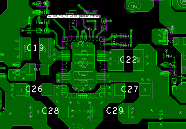
I have this design, in practice 3 parts failed  after a few days of work, showing short circuit at the output.

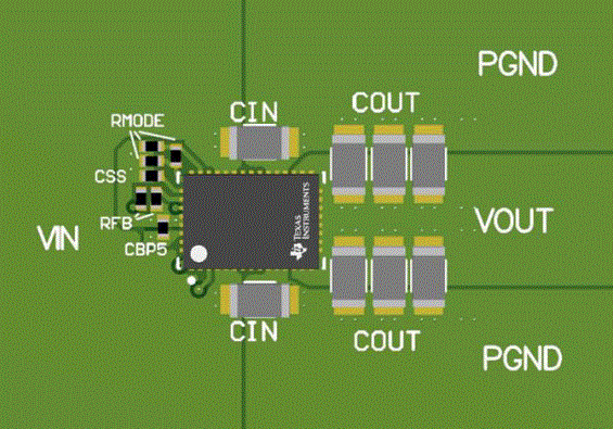
I have further investigated one part after removing from the board and VOUT2 (pins 13-19) are showing zero ohm to the center ground pad

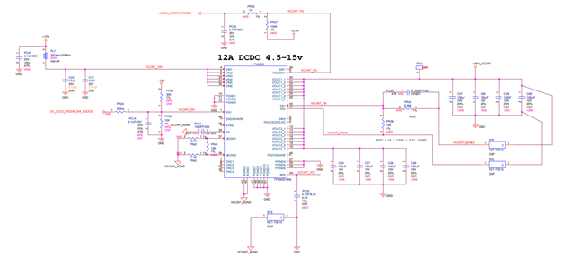
The input voltage is 12V

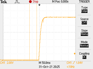
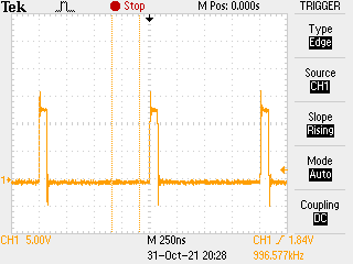
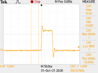
What could be the reason for the destruction of the parts?

  •   Do you have a pcb layout image that can be shared?

    If Vout2 pins are showing a low impedance to PGND pin, this implies a power stage or maybe capacitor failure.  Can you check the impedance from the SW2 (pin 9) to PGND (pin 49 or one of the adjacent pins) on the fail unit.  Check the SW1 to PGND for reference.

    On an device, that is/was operating do you have oscilloscope plot on the VIN (pins 4,5,6) to PGND (pins 10,11,12) or VIN (pins 33, 34, 35) to PGND (pins 27,28,29) or SWx to PGND pins.    

  • Hi,

    This is the layout snapshot

    As for the oscilloscope waveforms:

    Vin

    SW2 (SW1 looks the same):

  • Hi Amon

    Daniel is looking into this and will feedback to you soon.

    BR

    Ruby

  • The CIN capacitors need to be next to the VIN and PGND pins to minimize the inductance. 

    C19 near   pins 4 to 6 and pins 10 to 12

    C22 near  pins 33 to 35 and pins 27 to 29.

    The current layout has the CIN C19 capacitor connecting to PGND through vias which is not ideal.

    The long lines increases inductance, voltage ringing on the power stage. 

    The C22 is better but, can be improved 

    For troubleshooting purposes, Can the board be modified to place a capacitors next to the VIN and PGND pins and the tests rerun.