This thread has been locked.

If you have a related question, please click the "Ask a related question" button in the top right corner. The newly created question will be automatically linked to this question.

LM340: LM340S-12

Part Number: LM340

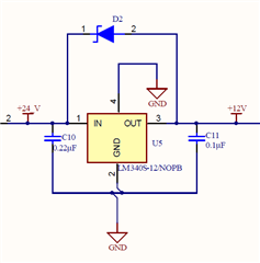
The datasheet of LM340S-12 says Dropout voltage is 2v, maximum input is 35V.

Can anyone help confirm is it ok if I use it in the circuit input 24V DC, output 12VDC, maximum load current 0.5A, and how to calulate the thermal /temperature rising? Thanks in advance!

  • Hello,

             Given that Vin = 24V, Vout = 12V and Load Current = 0.5A, the power dissipated across the die is 6W ((24V - 12V)*0.5A). The Junction to Ambient Thermal Resistance RθJA provided in the Datasheet relates Junction Temperature (TJ), Ambient Temperature (TA) and Power Dissipation (PD) as TJ = TA + PD*RθJA. Assuming that the Ambient Temperature is 25°C, its does appear that, for this level of power dissipation, the Junction temperature will exceed 125°C (since RθJA is at least 24°C/W). Could the input voltage be reduced? Thanks!

    Regards,

    Srikanth   

  • Hi Srikanth, thanks for your reply, we have a fixed power source of 24V, cannot change it. I saw the datasheet says maximum PD is 15W, and maximum TJ is 125 or 150 degree C, if TJ = TA + PD*RθJA, then PD(max)*RθJA will be higher than 300 C, this doesn't make sense, PDmax is too high.

    And if the PCB layout has a big aera copper (top and bottom side) for the LDO heatsink, can I keep the circuit ( Vin = 24V, Vout = 12V and Load Current = 0.5A,), i mean even the TJ is high, but can be dissipated by heatsink soon, does this work?

  • Hi Allen,

                 Increasing copper area would help, but only to an extent. Figures 29 and 31 of the datasheet indicate that increasing the copper area beyond 1 square inch does not result in any significant improvement in RθJA. The power dissipation would need to be less than 3W to ensure that the junction temperature does not exceed 125°C (as indicated by Figures 30 & 32). Could additional components be installed to step down the input voltage? Thanks!

    Regards,

    Srikanth

  • Hi Srikanth, thanks a lot for the clarification, the circuit can be modified to reduce 12V current to 43mA, then PD is around 0.71W, I think this will be safe.

    I have another question, maybe not related to the LDO, but it will be appreciated if you can help. As the attached picture , when 24V input shutdown, C11 discharges and C10 got charged via D2, if i don't consider the load on the right side of C11, how can I calcuate the Maximum forward current on D2? 

  • Hello,

             I am looking into this, I will get back to you by the end of the day tomorrow. 

    Regards,

    Srikanth

  • Hi Srikanth, 

    Thank you so much!

    Best Regards!

    Allen

  • Hello Allen,

                      There will be a forward current flowing through D2, only when it is forward biased (VOUT > VIN). This is an unlikely event (without an External Bias  or short to battery condition), as it requires C11 to retain its charge and only C10 discharge. Even if this event does occur, C11 would send a current to charge C10 as soon as D2 is even slightly forward biased. This process would continue until both capacitors discharge. In this scenario, I cant see the forward current assuming large values (it certainly would be much smaller than 1mA). The situation would be different if the output pin is shorted to battery (Vout > Vin). Hope this was help. Thanks!

    Regards,

    Srikanth    

  • Hi Srikanth, thanks a lot!