Other Parts Discussed in Thread: BQ76PL536EVM-3,
Hi Everyone
Im used a custom PCB based on BQ76PL536EVM-3 board, so the connections and SPI communications are fine.
Im using 2 BQ76PL536A-Q1 in daisy chain configuration (a microcontroller is the master and the 2 BQ's are the slaves).
I address correctly both ICs I can read properly its addresses, then I execute the configuration for each IC and then remove the faults and errors registers of each IC (device status 0x81).
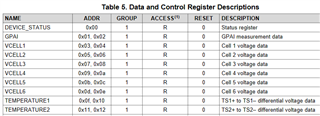
And the last step, when Im going to try to read the voltages of cells and temperatures, I can only read the first cell of each BQ and not the complete pack (0x00 is the responese for the rest of cells)
About the temperatures the same the answer is 0x00.
The rest of registers i can read em correctly like, status device, faults, errors, addres etc...
I dont know what try more, is very frustrating
I attach in this thread my configuration.
/**
*******************************************************************************
/fn					Configurado_BQ
/brief				Funcion para configuar correctamente 1 BQ, registros
 	 	 	 	 	y valores obtenidos tras depuracion de placa BQ76PL536EVM-3
 	 	 	 	 	con	SPI/USB Aadvark
/param[in]			N/A
/return				0 Direccionado en curso, 1 BQ direccionado
*******************************************************************************/

uint8_t Configurado_BQ 			(void){

	switch ( iME_0 )
	{

	case 0:				/**ADC_CONTROL_REG*/

	Write_SPI   (Broadcast, ADC_CONTROL_REG, 0x75);
	Read_1byte_SPI (Dir1, ADC_CONTROL_REG);

	if(Rx_Spi[3]==0x75){
		iME_0=1;//sig
		break;
	}else{
		iME_0=0;//act
		break;
	}

	case 1:				/*IO_CONTROL_REG*/

	Write_SPI   (Broadcast, IO_CONTROL_REG, 0x00);
	Read_1byte_SPI (Dir1, IO_CONTROL_REG);

	if(Rx_Spi[3]==0x00 && Rx_Spi[4]!=0x00){
		iME_0=2;//sig
		break;
	}else{
		iME_0=1;//act
		break;
	}

	case 2:				/*CB_CTRL_REG*/

	Write_SPI   (Broadcast, CB_CTRL_REG, 0x00);
	Read_1byte_SPI (Dir1, CB_CTRL_REG);

	if(Rx_Spi[3]==0x00 && Rx_Spi[4]!=0x00){
		iME_0=3;//sig
		break;
	}else{
		iME_0=2;//act
		break;
	}

	case 3:				/*CB_TIME_REG*/

	Write_SPI   (Broadcast, CB_CTRL_REG, 0x00);
	Read_1byte_SPI (Dir1, CB_TIME_REG);

	if(Rx_Spi[3]==0x00 && Rx_Spi[4]!=0x00){
		iME_0=4;//sig
		break;
	}else{
		iME_0=3;//act
		break;
	}

	case 4:				/*FUNCTION_CONFIG_REG*/

	Write_SPI 	(Broadcast, SHDW_CTRL_REG, 0x35);
	Write_SPI 	(Broadcast, FUNCTION_CONFIG_REG, 0x40);
	Read_1byte_SPI	(Dir1, FUNCTION_CONFIG_REG);

	if(Rx_Spi[3]==0x40){
		iME_0=5;//sig
		break;
	}else{
		iME_0=4;//act
		break;
	}

	case 5:				/*IO_CONFIG_REG*/

	Write_SPI 	(Broadcast, SHDW_CTRL_REG, 0x35);
	Write_SPI 	(Broadcast, IO_CONFIG_REG, 0x00);
	Read_1byte_SPI	(Dir1, IO_CONFIG_REG);

	if(Rx_Spi[3]==0x00 && Rx_Spi[4]!=0x00){
		iME_0=6;//sig
		break;
	}else{
		iME_0=5;//act
		break;
	}

	case 6:				/*CONFIG_COV_REG*/

	Write_SPI 	(Broadcast, SHDW_CTRL_REG, 0x35);
	Write_SPI 	(Broadcast, CONFIG_COV_REG, 0x80);
	Read_1byte_SPI	(Dir1, CONFIG_COV_REG);

	if(Rx_Spi[3]==0x80){
		iME_0=7;//sig
		break;
	}else{
		iME_0=6;//act
		break;
	}

	case 7:				/*CONFIG_COVT_REG*/

	Write_SPI 	(Broadcast, SHDW_CTRL_REG, 0x35);
	Write_SPI 	(Broadcast, CONFIG_COVT_REG, 0x00);
	Read_1byte_SPI	(Dir1, CONFIG_COVT_REG);

	if(Rx_Spi[3]==0x00 && Rx_Spi[4]!=0x00){
		iME_0=8;//sig
		break;
	}else{
		iME_0=7;//act
		break;
	}

	case 8:				/*CONFIG_CUV_REG*/

	Write_SPI 	(Broadcast, SHDW_CTRL_REG, 0x35);
	Write_SPI 	(Broadcast, CONFIG_CUV_REG, 0x80);
	Read_1byte_SPI	(Dir1, CONFIG_CUV_REG);

	if(Rx_Spi[3]==0x80){
		iME_0=9;//sig
		break;
	}else{
		iME_0=8;//act
		break;
	}

	case 9:				/*CONFIG_CUVT_REG*/

	Write_SPI 	(Broadcast, SHDW_CTRL_REG, 0x35);
	Write_SPI 	(Broadcast, CONFIG_CUVT_REG, 0x00);
	Read_1byte_SPI	(Dir1, CONFIG_CUVT_REG);

	if(Rx_Spi[3]==0x00 && Rx_Spi[4]!=0x00){
		iME_0=10;//sig
		break;
	}else{
		iME_0=9;//act
		break;
	}

	case 10:				/*CONFIG_OT_REG*/

	Write_SPI 	(Broadcast, SHDW_CTRL_REG, 0x35);
	Write_SPI 	(Broadcast, CONFIG_OT_REG, 0x00);
	Read_1byte_SPI	(Dir1, CONFIG_OT_REG);

	if(Rx_Spi[3]==0x00 && Rx_Spi[4]!=0x00){
		iME_0=11;//sig
		break;
	}else{
		iME_0=10;//act
		break;
	}

	case 11:				/*CONFIG_OTT_REG*/

	Write_SPI 	(Broadcast, SHDW_CTRL_REG, 0x35);
	Write_SPI 	(Broadcast, CONFIG_OTT_REG, 0x00);
	Read_1byte_SPI	(Dir1, CONFIG_OTT_REG);

	if(Rx_Spi[3]==0x00 && Rx_Spi[4]!=0x00){
		iME_0=12;//sig
		break;
	}else{
		iME_0=11;//act
		break;
	}

	case 12:				/*LIMPIEZA ALERT y FAULTS*/

	Write_SPI 	(Broadcast, FAULT_STATUS_REG, 0xFF);
	Write_SPI 	(Broadcast, FAULT_STATUS_REG, 0x00);
	Write_SPI 	(Broadcast, ALERT_STATUS_REG, 0xFF);
	Write_SPI 	(Broadcast, ALERT_STATUS_REG, 0x00);
	Read_1byte_SPI	(Dir1, DEVICE_STATUS_REG);

	if(Rx_Spi[3]==0x81){
		iME_0=13;//sig
		break;
	}else{
		iME_0=12;//act
		break;
	}

}//Fin switch

	if(iME_0 == 13){
	iME_0=0;
	return 1;	// Configurado Correcto
	}
	return 0;	// Configurado en Curso
}
Many thanks in advance!