This thread has been locked.

If you have a related question, please click the "Ask a related question" button in the top right corner. The newly created question will be automatically linked to this question.

UCC27524A1-Q1: Which current does "500-mA reverse current without either damage" mention and why should this limitation be considered?

Part Number: UCC27524A1-Q1

Hi team, 

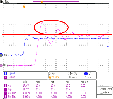
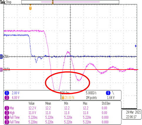
Which current does "500-mA reverse current without either damage", which is written in its datasheet "8.3.4 Output Stage", mention and why should this limitation be considered?

UCC27524A1-Q1 could sink and source 5A but this datasheet mentions 500-mA reverse current limitation and I cannot understand which reverse current I should take care and why damage could happen be this event. Is it related to latch up tolerance or something different? Explanation for "which current reverse current mentions" with "Figure 20. UCC27524A1-Q1 Gate Driver Output Structure" could be helpful for my understanding.

If this "reverse current" mentions external MOSFET driven by UCC27524A1-Q1, then negative pulse occur and maybe lead latch-up. In this case, is this reverse current limitation depending on "external MOSFET body diode characteristics" or "how much negative pulse happen on external MOSFET drain-source involved with UCC27524A1-Q1 OUTx to GND negative voltage"?

Regards,
Ochi

  • Hello Ochi,

    The datasheet is referring to a current imposed on the driver output that is in the reverse direction of the driver output state. For example if the driver is high normally sourcing current the reverse would be a transient in the driver output causing the driver to sink current. And the opposite in the case of a driver low state, when the driver normally is sinking current (low) it can source current to the 500mA level.

    This would normally be encountered with driver output voltage transients.

    Regards,

  • Hi Richard, 

    Could you please show me the driver output waveforms example and why this reverse current happen on sink/source transient?

    Regards,
    Ochi

  • Hi Ochi-san,

    Large current spikes (di/dt) into GND from switching of the power stage can cause GND noise that gets coupled into the driver outputs (through the C_gs and C_gd parasitic capacitances).

    Current will flow through the body diodes of the internal FETs of the driver anytime the output of the driver is a diode drop above VDD or a diode drop below GND.  These conditions are typically due to overshoot or undershoot on the output.

    These waveforms below show typical overshoot and undershoot during turn-on and turn-off.

    OVERSHOOT:  When the output of the driver goes above the supplied VDD voltage, and the High-Side FET, body diode (internal to the driver) conducts the reverse current.

    UNDERSHOOT:  When the output of the driver goes below GND, and the Low-Side FET body diode (internal to the driver) conducts the reverse current.

    NOTE:  These waveforms are from a NON-TI device to show excessive overshoot and undershoot.

    I hope this this clarifies things for you!  If so, please press the green button, otherwise, feel free to follow up with additional questions.

    Thanks!

    Aaron Grgurich