This thread has been locked.

If you have a related question, please click the "Ask a related question" button in the top right corner. The newly created question will be automatically linked to this question.

TPS54386-Q1: TPS54386-Q1

Part Number: TPS54386-Q1
Other Parts Discussed in Thread: TPS54386

Hello

Regarding the TPS54386-Q1, the buyer is requesting a response from the supplier.

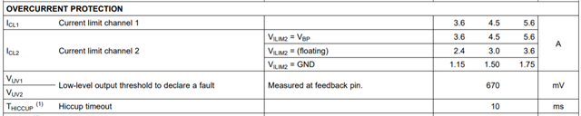
Currently I am using 3.3V output for SW1 part.

During the load test, when a load of about 1.6A is input to the 3.3V line, the protection circuit works when the voltage drops to 2.8V, and it was confirmed that the two channels enter the protection state.

There is a question about why the protection circuit operates at 1.6A when the maximum available current is 3.6A.

I explained that the TPS54386 IC detects and operates an externally input load, but the buyer does not understand.

Can you answer this question?

thank you.

  • Please change the C3 and C7 to 47nF, then test again. 

  • Hello

    Thank you for answer.

    Excuse me, but can you explain the principle of tps54386 ic entering protected mode?

  • Hello 

    "it was confirmed that the two channels enter the protection state

    [Zhao] Do you know what protection IC triggered? 

    I review the schematic, I found one error, C3 and C7 should be 47nF, not 334pF, which will cause IC cannot fully turn on High-side FET, maybe cause IC triggered over current protection. 

  • I put a load of about 1.6A on the 3.3v line, and the voltage on the 3.3V line goes down to about 2.8V and then down to 0.1V. Both channels were confirmed to be inactive. I thought this was the protection state of the IC.

  • It looks IC triggered over current protection. 

    Did you ever test the inductor current? we can check if it triggers OC limit. 

    If you have opportunity, suggest measuring some waveforms including SW1, BOOT1, Vout, and inductor current. 

    Besides, the solution is change C3 and C7 to 47nF as TI recommended. 

  • Yes, I will change it to 47nF and test it.

    If so, is it wrong for the protection circuit to operate when a 1.6A load is input to the 3.3V line?

    6.8uH inductor specification sheet.

    감사합니다.

  • As I mentioned, due to C3 and C7 value is not correct, which would cause IC cannot fully turn on High-side FET and FET Rdson is big, then would cause IC triggered over current protection. 

    Again, the problem is at C3 and C7 wrong value, not at IC.  

  • I changed C3 and C7 to 47nF and conducted the test.

    The protection circuit is now activated at 2.3A.

  • Hello 

    Did you measure the inductor current? 

    I check the inductor's saturation current, it is only 2.1A, so the inductor must be saturated. 

    Could you change another inductor with high saturated current? and then test again. 

  • The current inductor's normal load current is only 87mA.

    Assuming an external overcurrent condition in the load test, we are checking to what extent the protection circuit operates under the load.

    It's just that the buyer doesn't understand the mechanism that the protection circuit works.

  • Ok. 

    1. "47nF for C3 and C7 can improve the loading to 2.3A" --> this has proved my assumption:  

    IC cannot fully turn on High-side FET and FET Rdson is big, then would cause IC triggered over current protection. 

    2. Why it is only 2.3A? --> this might be caused by inductor saturated current.   

  • thank you.

    If so, can you explain the part where the protection circuit works when the voltage in the data sheet goes down???

    Output Overload Protection
    In the event of an overcurrent during soft-start on either output (such as starting into an output short), pulse-bypulse
    current limiting and PWM frequency division are in effect for that output until the internal soft-start timer
    ends. At the end of the soft-start time, a UV condition is declared and a fault is declared. During this fault
    condition, both PWM outputs are disabled and the small pulldown MOSFETs (from SWx to GND) are turned ON.
    This process ensures that both outputs discharge to GND in the event that overcurrent is on one output while the
    other is not loaded. The converter then enters a hiccup-mode time-out before attempting to restart. Frequency
    division means if an overcurrent pulse is detected, six clock cycles are skipped before the next PWM pulse is
    initiated, effectively dividing the operating frequency by six and preventing excessive current buildup in the
    inductor.
    In the event of an overcurrent on either output after the output reaches regulation, pulse-by-pulse current limit is
    in effect for that output. In addition, an output undervoltage (UV) comparator monitors the FBx voltage (that
    follows the output voltage) to declare a fault if the output drops below 85% of regulation. During this fault
    condition, both PWM outputs are disabled and the small pulldown MOSFETs (from SWx to GND) are turned ON.
    This design ensures that both outputs discharge to GND, in the event that overcurrent is on one output while the
    other is not loaded. The converter then enters a hiccup-mode timeout before attempting to restart.
    The overcurrent threshold for output 1 is set nominally at 4.5 A. The overcurrent level of output 2 is determined
    by the state of the ILIM2 pin. The ILIM setting of output 2 is not latched in place and may be changed during
    operation of the converter.

  • Simply speaking, when C3 and C7 are small, the high-side FET cannot be fully turn on, which means their Rdson are large, when adding loading, the voltage drop on high-side FET become large, so the Vout drops and trigger UVP. 

  • thank you.

    I've been a really great help.