This thread has been locked.

If you have a related question, please click the "Ask a related question" button in the top right corner. The newly created question will be automatically linked to this question.

BQ25125: VSYS output 3.3V

Part Number: BQ25125

Hi !

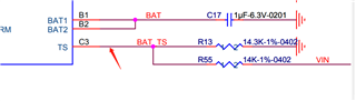
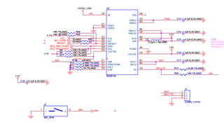
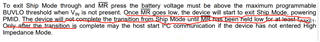
      We set the VSYS output to 3.3V.  By setting register 0x6 to 0xfe.  When we exit shipmode using the following method, the VSYS output is not 3.3V, but 1.8V.  We want to know what might cause this setting to fail?

  • Hi Guanghua, 

    That behavior is expected, once you enter shipmode the registers will get reset to the default values. The default SYS value is 1.8V. You will need to reconfigure the registers after exiting ship mode. 

    As a good resource you can refer to the below link which has a list of common questions and answers about the BQ25125 device. 

    BQ2512x FAQs: https://www.ti.com/lit/pdf/sluaah8

    Best regards, 

    Arelis G. Guerrero 

  • Hi Arelis G. Guerrero !

         Exit shipMode and we re-initialize 0x6 to 0xfe. However, we found that 3.3V was related to the input battery voltage.  When the battery voltage is below 3.7V, VSYS 3.3V input should wait until 0x6 is set to 0xfe 30 seconds later. We don't know why, but what is the relationship between the VSYS 3.3V output and the battery input voltage?

  • Hi Arelis G. Guerrero !

             The battery we choose has no temperature detection function. As shown below, will this design of our TS pin affect the normal operation of 25125? Thank you!

  • Hi Guanghua, 

    Can you clarify the following statement? 

    Exit shipMode and we re-initialize 0x6 to 0xfe. However, we found that 3.3V was related to the input battery voltage.  When the battery voltage is below 3.7V, VSYS 3.3V input should wait until 0x6 is set to 0xfe 30 seconds later. We don't know why, but what is the relationship between the VSYS 3.3V output and the battery input voltage?

    Also, do you have a scope capture with the waveform you are seeing from exiting shipmode, programming, and SYS output (VBAT, VIN, SYS, and MR)? Can you also provide the charger portion of your schematic? 

    he battery we choose has no temperature detection function. As shown below, will this design of our TS pin affect the normal operation of 25125? Thank you!

    For the TS question. If not using this function we recommend putting the TS above the TSOFF (TS Disable threshold). To be in that range you will need to swap R55 to be around 9k. You want more than 60% of VIN on the TS pin on the resistor divider, right now you are ~=50.5%. 

    Best regards, 

    Arelis G. Guerrero 

  • Hi Arelis G. Guerrero,

           1、Below is our schematic diagram.VBAT is 3.76V, no USB is inserted,VIN does not provide input, MR is pulled down about 500ms and then pulled up, SYS is set 0x6 to 0xFE, keep 1.8V and change to 3.3V about 30S later.


         2、We have known the TS question, thank you。

    Best regards, 

     Guanghua

  • Hi Guanghua, 

    Thanks for providing the schematic. The MR input has an internal pull-up to battery. How is the MR being driven low? Is the MR directly connected to your MCU? or is there an NMOS or something in between? Do you happen to have a scope capture of the behavior you are observing? 

    Best regards, 

    Arelis G. Guerrero 

  • Hi Arelis G. Guerrero,

         MR connects the key through an ESD as shown below.  We tried to capture the waveform, but we didn't get it with some difficulty.  The test results show that SYS V3.3 is related to the power supply battery voltage.  We want to know what is this relationship?  At what low battery voltage does the SYS theoretically fail to output 3.3V?  


    Best regards,

    Guanghua Guo

  • Hi Guanghua, 

    There should not be a voltage of BAT that would make the SYS to fail. As long as BAT > BATUVLO and the I2C communication is successful (ACK), you should be able to change the SYS voltage. However typically you want to have some headroom, the D/S recommend having VPMID > VSYS + 0.7V for optimal operation. It'll be good to see some scope captures of this, to see if the BAT is being dropped below BATUVLO at any point, causing a reset event. 

    The MR pin has an internal pull-up to battery, it appears you are driving the MR with your MCU. What is the logic level of your MCU rail? You could be violating the IO pins abs max of your microcontroller or not meeting the logic level of your MCU.  You can refer to this post for an alternative way on how to drive this pin with your MCU. https://e2e.ti.com/support/power-management-group/power-management/f/power-management-forum/1047309/faq-bq25120a-can-i-drive-the-mr-pin-externally-through-a-gpio

    It'll be good to know at what battery voltage level you are seeing this behavior? And if you can confirm the I2C communication was successful? Can you provide the register dumps when it fails (before and after programming the SYS voltage)? And also if you could provide the scope capture with the waveform you are seeing from exiting shipmode, programming, and SYS output (VBAT, VIN, SYS, and MR)? 

    Best regards, 

    Arelis Guerrero 

  • Hi Arelis Guerrero.

       According to your suggestion the D/S recommend having VPMID > VSYS + 0.7V for Optimal operation. Our test found that the battery was 3.12V, VPMID was 0.79V and VSYS was 0V. What are the possible causes? We believe that VPMID should be basically equal to the battery voltage, no matter what the situation is.

    Best regards, 

    Arelis Guerrero