Other Parts Discussed in Thread: UCC24650
Hello
I tried looking around at some previous forum posts and SLUAAC5 "Flyback Aux Winding OVP and UVLO Fault Sensing Design and Troubleshooting Tips" (https://www.ti.com/lit/an/sluaac5/sluaac5.pdf) and can't seem to find my issue or the resolution.
I'm trying to implement the UCC28730 in a DC-DC converter with ultra-low standby. Targeting operation at 250VDC to 450VDC in and ~5.5V out (for LDO regulation to 5V then 3.3V and 1.2V for MCUs).
[See Spreadsheet]
The schematic for the circuit is above. The UCC24650 has been removed for testing.
RS1 (R2) = 100k, RS2 (R7) = 30k, which should give me OVP threshold of ~7.1 OVP and Regulated Vout of ~ 6.2V according to SLUC579. Transformer datasheet here: au.mouser.com/.../760875112-1724366.pdf
Testing is mostly being done with 250VDC in. Some quick tests with 300VDC in didn't seem to have much of an effect. Startup voltage seems to be ~220VDC.
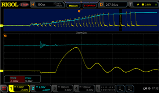
The device seems to be going into a fault state as evident by the VDD oscillating between the ~7V and ~21V UVLO on/off voltages and there is unacceptable output voltage regulation with overvoltage and excessive ripple.
CH1 is VDD to HV-. CH2 is Vout (LV+ to LV-)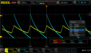
10k ohm output load. 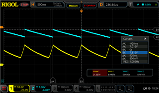
100k ohm output load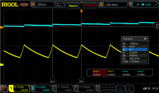
1 Meg ohm output load.
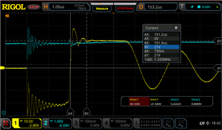
Zooming into the turn on transient, the VS seemed to be going over the 4.6V threshold for 3 consecutive cycles, causing OVP shutdown. Note there is some changing of the load values which affected the number of cycles but the waveform shapes and amplitude before shutdown where the same.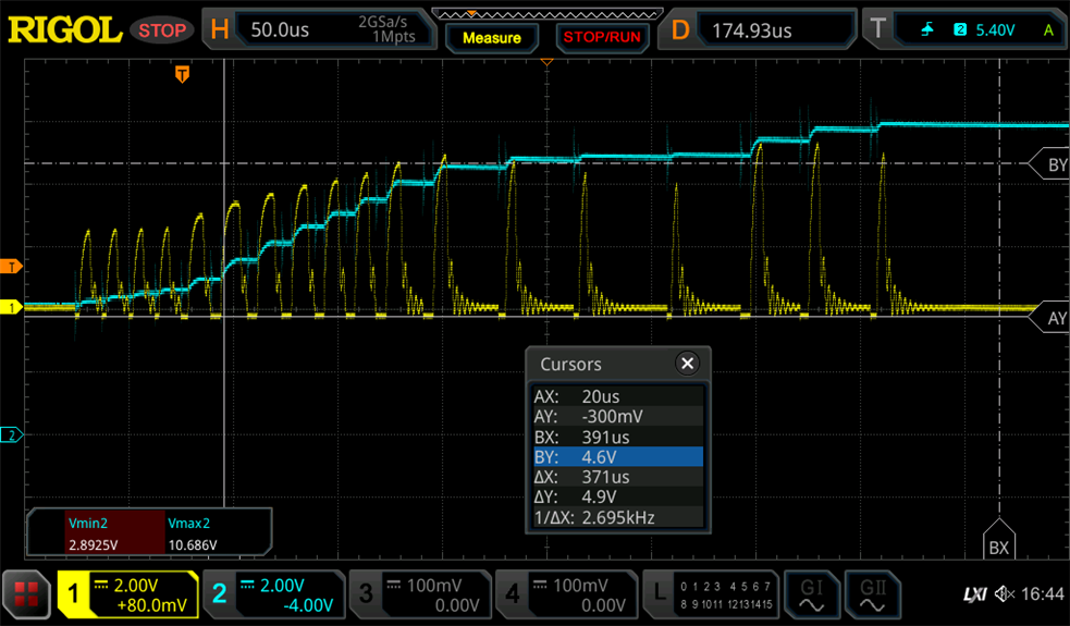
10k ohm load. CH1 is VS (probed with a x1 passive probe, 50pF +/-20pF) CH2 is Vout
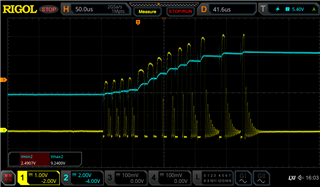
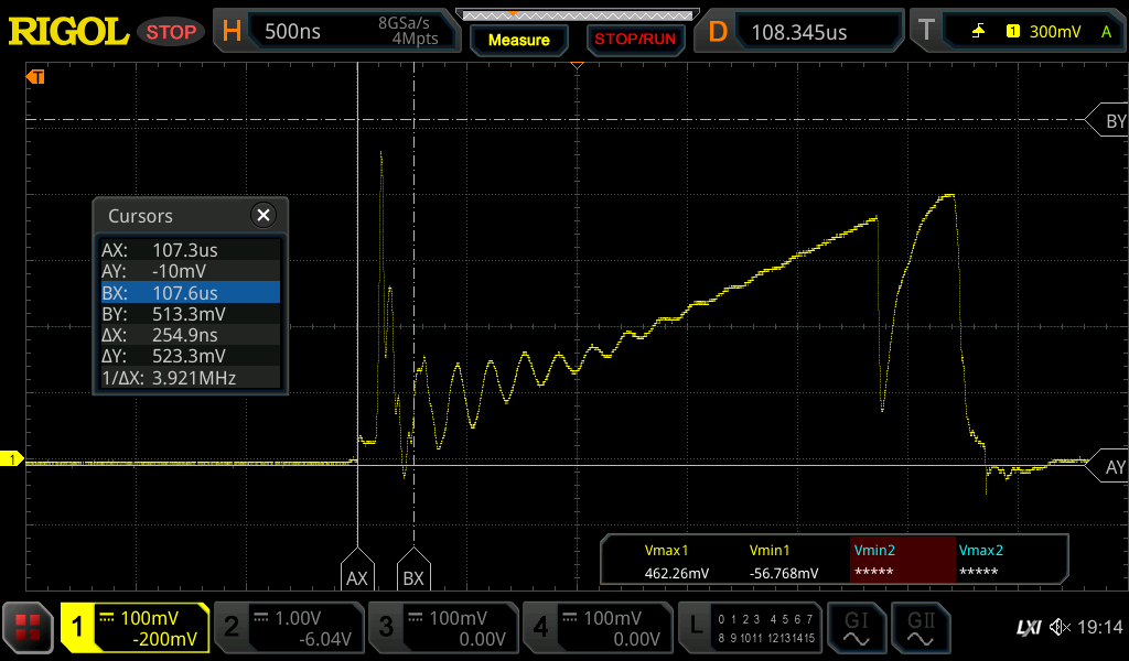
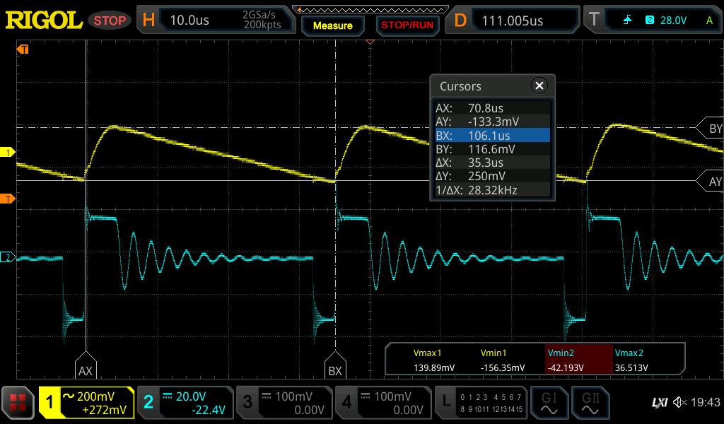
10k ohm load. CH1 is VS (probed with a x10 passive probe, 20pF +/-5pF) CH2 is Vout
I also checked for other potential fault conditions. As mentioned above, increasing the input voltage didn't seem to change anything.
Checked if the VDD cap is insufficient and dropping voltage triggering UVLO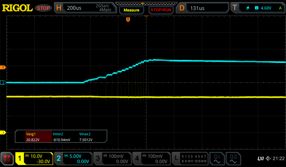
CH1 VDD, CH2 Vout. VDD does not appear to be getting exhausted and triggering a UVLO.
OCP also does not appear to be the issue.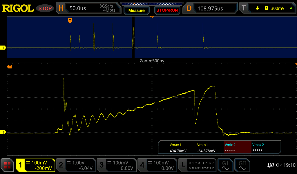
100k ohm load. CH1 is voltage across the current sense resistor (my R6= 1 ohm). The peak voltage observed is ~510mV ->510mA i.e. well below 1.5V OCP threshold.
The gate drive transient also appears to be well within the current sense leading edge blanking time (t_CSLEB=250nS). There also does not appear to be excessive or superfluous noise.
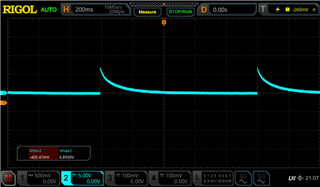
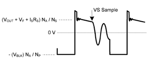
Taking a closer look at the Auxiliary winding waveform as recommended in documents now: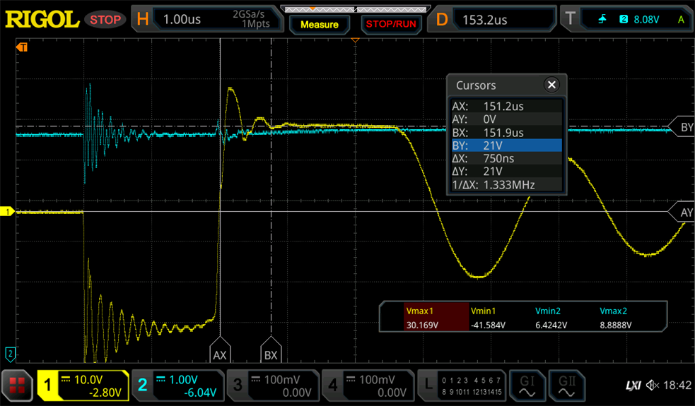
100k ohm load. CH1 is AUX (Aux diode D5 anode to HV-). CH2 is Vout.
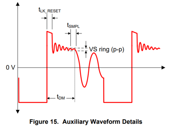
There does not appear to be excessive noise or ringing on the auxiliary waveform (apart from aux diode reverse bias ringing). The leakage inductance ripple/plateau appears to be sufficiently past the minimum. t_(LK_RESET)=750ns.
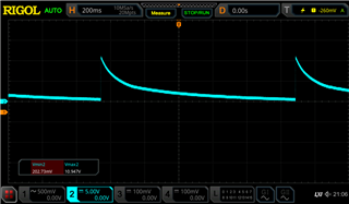
Taking a closer look at VS in the cycle before output voltage overshooting occurs:
CH1 VS, CH2 Vout. (x1 probing?)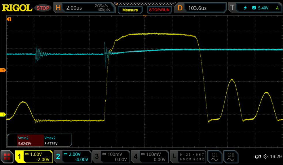
CH1 VS, CH2 Vout. (x10 probing)
The feedback signal looks quite "soft" with a very slow capacitive rise. This is likely due in part to probe loading but I wonder if this could be the issue, excess rise time on the VS pin causing issues in the output voltage measurement and overshooting into OVP. My only idea right now is to try adding capacitive bypassing to the VS voltage divider to try improve the VS frequency response but that could potentially cause more complications.
I am able to get it to run in light DCM without faults occurring (no VDD oscillation and good regulation) but this requires a relatively high load of 10 ohms (Vout ~6.6V, Iout 660mA) and this was fairly unstable with the switching period varying quite a bit and sometimes slipping back into the fault condition. Values from 10k ohm through 10 ohm (using a decade box) were also tested but it did not seem to operate without faults until ~10ohm load.
10 ohm load. CH1 Vout, CH2 Aux winding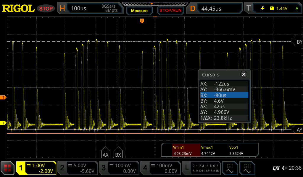
9 Ohm load. CH1 VS.