This thread has been locked.

If you have a related question, please click the "Ask a related question" button in the top right corner. The newly created question will be automatically linked to this question.

CSD25304W1015: MOSFET Vgs Max

Part Number: CSD25304W1015
Other Parts Discussed in Thread: CSD25211W1015

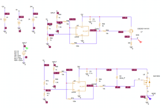
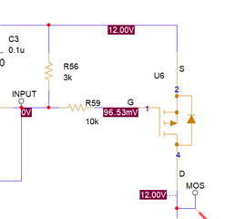
Hi, I am using a MOSFET as switch, as the attached circuit, MOSFET on when input is 0V, and off when input is 12V.

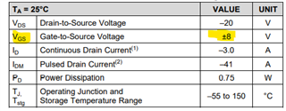
I have a question, the datasheet mentions Vgs Max is +/-8V, looks in my circuit Vgs will be -12V when input is 0V. Does this mean it's risk to damage MOSFET, and what should be the input voltage safe for this case?

Any comments will be appreciated.


CSD25304W1015

  • Hello Allen,

    Thanks for your interest in TI FETs. Exceeding the abs max rating of VGS can damage the FET and TI cannot guarantee its reliability. You should never exceed the absolute maximum rating specified in the MOSFET datasheet. You will need to modify your design to limit the maximum VGS. For example, you can add a zener diode from gate-to-source to clamp VGS <= +/-8V. Can you share your simulation file with me? We have another device, CSD25211W1015 in the same footprint that includes a gate-source ESD diode that behaves like a 6.3V zener diode. I would like to run some simulations with that device.

    Best Regards,

    John Wallace

  • Hi John, thanks a lot for your reply, I put CSD25211W1015 in the simulation, but saw there is spike in the waveform, could you have a look how to avoid it.

    Attached is the simulation file, we have another circuit MOSFET working voltage is 24V, I placed a 19V zener between S and G gate, to avoid VGS exceed 20V limitation.

    Please help advice is there any issue in the circuit.

    KVM.zip

  • Hi Allen,

    I will take a look at your simulation. I think the best way to avoid exceeding abs max VGS is to add a zener diode between gate and source. The CSD25211W1015 integrated gate ESD diode was characterized during product development but has not been tested in an application where it was used to clamp the gate voltage during continuous operation. Therefore, I think it's best to continue using the CSD25304W1015 with added zener diode between gate and source.

    Best Regards,

    John

  • Hi John, got it. the zener diode is required between G and S gate to clamp the VGS. Thanks a lot.