This thread has been locked.

If you have a related question, please click the "Ask a related question" button in the top right corner. The newly created question will be automatically linked to this question.

TPS65185: TPS65185

Part Number: TPS65185

Hi E2E,

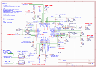
May I ask for an E2E design review of this TPS65185?

This is intended for a 4-layer, single-sided PCB.

Review requested:

* Any errors, omissions, duplicates?

* Sources - 3.7V LiPo VBAT source, and 3.3V source from load switches.  All okay?

* Values - cap voltages, inductors, etc

* Cap types - caps mlcc vs tantalum?

* Power plane stack-up suggestions (constrained to single-sided only)

Many thanks!

Will

  • Hi,

    Regarding your questions:

    1. See schematic review comments below.
    2. A battery is acceptable for VIN and load switches for supply delivery is acceptable. I suggest checking if the load switches recommend input/output capacitors.
    3. See schematic review comments below.
    4. MLCC capacitors are recommended for this device.
    5. The stackup for a 4-layer single-sided board should be similar to the EVM.
      • Top layer: components
      • Mid layer 1: continuous GND plane
      • Mid layer 2: power planes and routing
      • Bottom layer: GND and routing

    Comments on the schematic:

    • nINT is open-drain and requires a pull-up resistor
    • 10 uF decoupling capacitor is recommended close to the VIN pin
    • 4.7 uF decoupling capacitor is recommended close to the VCOM_PWR pin
    • PWR_GOOD is open-drain and requires a pull-up resistor
    • 10 uF decoupling capacitor is recommended close to the VIN_P pin
    • AGND and DGND are not connected on this sheet
  • Yes, thank you E2E.  I did have the pullups and decoupling on another page - I have since relocated those on the schematic to improve readability.  I'm good here. Thank you E2Eers!