This thread has been locked.

If you have a related question, please click the "Ask a related question" button in the top right corner. The newly created question will be automatically linked to this question.

TPS561208: Switching layout guidelines

Part Number: TPS561208
Other Parts Discussed in Thread: TPS563202EVM

Hi,

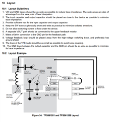
on the SPEC in section 10.1 it is recommended not to route the switching under the device.
can help to elaborate more why it is not recommended?   

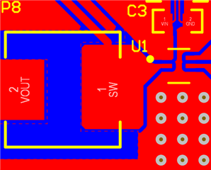
in my design i've routed it beneath the IC to minimize the SW line and not to route it with VIAs in more than one layer:

SW - purple, GND- yellow, Vin - Blue, Vout - Orange

can help to review layout and advise how crucial it is to fix?

have to say that design was checked (@ -40C, @25C, @105C) for ripples, current transients, wake-ups, efficiency, load regulation, voltage regulation - no issues found.

Thanks, 

Uri 

  • Hi Uri!

    When SW area be under IC, the parasitic capacitance between other electrical nodes and SW will be large.

    The larger the SW area, the larger the capacitance. The switch node has a high-speed-changing voltage, which means high du/dt. From theory i=c*du/dt, there may be leak current through SW and other electrical node of IC, which may cause noise and disturbing the normal operation.  So it is not recommended designer to do that.
    The above is just analysis the issue possibility of SW under device.
    The schematic and layout have been reviewed. Besides SW item, other parts are no problem.
    Shuai
  • Hi Shuai,

    thanks alot for your response.

    Just to make sure i've understood correctly, we are concerned from parasitic capacitance between switching node and the IC, correct?
    my PCB is 6 layers, how many VIAs you recommend me to use when im routing the switching node from bottom to top? what is the distance i need to save from those VIAs in internal layers? what is the distance need to save on the switching node on the opponent side of the PCB? 

    Thanks,

    Uri

  • Hi

    (1) Your understand is right.

    (2) Actually, it is not recommend using via to connect SW in different layers. Especially, in high current condition.

    You can refer the following layout. The left side is VIN, SW, and GND.

    Shuai

  • Hi,

    can share full layout guidelines? 
    from SPEC i only can see below image and guidelines:
     

    Thanks,

    Uri

  • Hi

    Yes, this is the early guide. It has some shortage.

    Now we recommend the layout show as last reply.  You can also refer the TPS563202EVM's user' guide.

    Shuai

  • Hi,

    thanks for your answer.

    routing back the GND from output capacitors to input capacitors is allowed under the IC?

    what about routing the SW node to capacitor of BST pin? can be routed in internal layer? what is the distance to save from other nets?

    thanks,

    Uri

  • Hi

    (1) Yes. This way is widely used in our EVM.

    (2) You mean routing SW under C_BST?  It is no problem.

    It recommend 35mil in the same plane.

    Shuai