This thread has been locked.
If you have a related question, please click the "Ask a related question" button in the top right corner. The newly created question will be automatically linked to this question.
ALL HI!
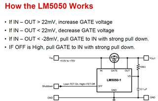
I want to use lm5050-1 as a switch control after DCDC output. Because the output end of DCDC power supply is connected with farad capacitor, if DCDC suddenly loses power, a reverse voltage will be connected to the output end of DCDC, resulting in damage to DCDC chip. Therefore, lm5050-1 is used for reverse current isolation. But I don't quite understand the principle of lm5050-1 reverse blocking current. Please Ti engineer to explain. As shown in the figure below, how does the comparator block the reverse current?thank you!
Hi Sheng,
The working of reverse current protection functionality in LM5050-1 is pretty simple. When ever the input (IN) voltage falls below output (OUT) by 28 mV (which is the VSD(REV)), the Gate is pulled low there by turning OFF the Mosfet. The turned OFF Mosfet blocks reverse current.
For more understanding, please refer to section '7.3.1 IN, GATE, and OUT Pins' of the datasheet.
HI!Praveen GD !
When lm5050-1-q1 drives the field tube, the maximum forward current is 15A. If the current is too large, can it carry out the function of overcurrent protection? If there is no overcurrent protection, how can I ensure that high current does not damage the chip?
Hi Sheng,
LM5050-1 is an ORing controller and hence it only offers reverse current protection.
In case you want reverse current protection + Over current protection, the best solution we can offer right now with Automotive Qualified parts is as shown in figure below.
For more understanding, please refer to section 'Design # 4: Reverse Battery Protection With Overcurrent Protection' of App note