This thread has been locked.

If you have a related question, please click the "Ask a related question" button in the top right corner. The newly created question will be automatically linked to this question.

TPS1HB08-Q1: Schematic Review Support

Part Number: TPS1HB08-Q1

Dear Support Team, 

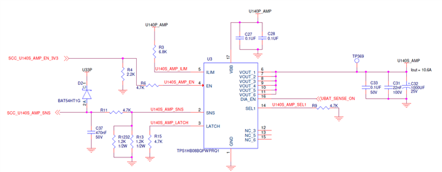
As per TI recommendation We have changed the high current part TPS1HB08-Q1 load switch in design, I would like to get your support to review the schematic. Please look into it and provide your feedback

Input = 14V

Output= 14V

Iout = 10.6A

Regards,

Bala

  • Hi Bala,

    I have a couple comments regarding the schematics:

    1. Protection resistor can be placed at DIA_EN pin to protect microcontroller from reverse current events.

    2. Is the purpose of the D2 to clamp the voltage to 3.3V? If so, the forward voltage drop will cause the node to rise up to 4V and it may damage the microcontroller.

    3. A GND network can be considered to protect reverse polarity events. You can find more information about GND network on datasheet or https://www.ti.com/lit/an/slvae55/slvae55.pdf this app note.

    Regards,

    Yichi