This thread has been locked.

If you have a related question, please click the "Ask a related question" button in the top right corner. The newly created question will be automatically linked to this question.

TPS650330-Q1: Programming with MSP430F5529 LaunchPad FAILED

Part Number: TPS650330-Q1
Other Parts Discussed in Thread: MSP430F5529, , BOOSTXL-TPS65033

Good morning,

I am working with a MSP430F5529 LaunchPad trying to program the PMIC TPS650330-Q1.

https://www.ti.com/tool/BOOSTXL-TPS65033#overview

https://www.ti.com/tool/MSP-EXP430F5529LP

I was able to program without problems a TPS650330-Q1 that was found already in the Sockel of the BOOSTXL- TPS65033 board.

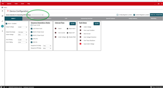
As soon as I insert one of the TPS650330-Q1 that I bought, I am not able to program them, not even possible to select the device (highlighted with green circle in the picture below).

I already performed/checked the following steps:

  • MCU firmware is up to date by clicking File > Program device in the GUI - see section 3.1.3 of the BOOSTXL-TPS65033 User's Guide: https://www.ti.com/lit/ug/slvubo3a/slvubo3a.pdf
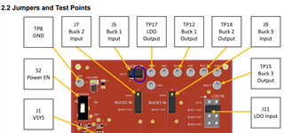
  • Device orientation - pin 1 should be located in the bottom left corner of the BoosterPack
  • J1 (VSYS), J5 (BUCK 1 IN), J12 (VIO) are all populated
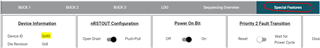
  • S1 (SEQ) is set to ON
  • VSYS ~= 5 V
  • VIO ~= 3.3 V

And, again, I CAN program the PMIC that was in the Sockel, unfortunately not the ones I received (PTPS65033007RGERQ1).

Any help/suggestion ist really appreciated!

Thank you very much

Best regards,

Leonardo

  • Hi Leonardo,

    Can you please share the register dump of the PTPS65033007RGERQ1 parts that you have received?

    You can export this as a JSON file by clicking File > Save Settings (top left corner of the GUI) with a connected device. 

    Thanks,

    Gerard

  • Hallo Gerard,

    Please find below the requested file. Unfortunately, I was not able to upload the .json file. Sorry about that.

    Thany you!
    Regards

    Leonardo


        "my_model": {
            "$refresh_interval": -1,
            "PID": 151,
            "RID": 8,
            "CONTROL_LOCK": 0,
            "BUCK_LDO_CTRL": 31,
            "GPIO_CTRL": 31,
            "CONFIG_LOCK": 0,
            "LDO_GPIO_CFG": 25,
            "BUCK1_VOUT": 16,
            "BUCK1_UVLO": 69,
            "BUCK2_VOUT": 10,
            "BUCK3_VOUT": 29,
            "LDO_VOUT": 18,
            "DISCHARGE_SETTING": 85,
            "SEQ_TRIG_BUCK1": 31,
            "SEQ_TRIG_BUCK2": 19,
            "SEQ_TRIG_BUCK3": 27,
            "SEQ_TRIG_LDO": 3,
            "SEQ_TRIG_nRSTOUT": 3,
            "SEQ_TRIG_GPIO": 63,
            "BUCK1_SEQ_DLY": 82,
            "BUCK2_SEQ_DLY": 50,
            "BUCK3_SEQ_DLY": 66,
            "LDO_SEQ_DLY": 34,
            "nRSTOUT_SEQ_DLY": 19,
            "GPIO_SEQ_DLY": 64,
            "INT_ACK": 0,
            "INT_ACK_BUCK1": 0,
            "INT_ACK_BUCK2": 0,
            "INT_ACK_BUCK3": 0,
            "INT_ACK_LDO": 0,
            "INT_MASK_BUCKx_LDO": 255,
            "FAULT_STATUS_BUCK1": 64,
            "FAULT_STATUS_BUCK2": 0,
            "FAULT_STATUS_BUCK3": 0,
            "FAULT_STATUS_LDO": 0,
            "VMON_BUCK1_CFG": 0,
            "VMON_BUCK2_CFG": 0,
            "VMON_BUCK3_CFG": 0,
            "VMON_LDO_CFG": 0,
            "ERR_BUCKx_LDO_CFG": 0,
            "RESTART_CMD": 0,
            "CFG_REG_CRC": 214,
            "DEV_STAT": 14,
            "POWER_GOOD_STATUS": 16,
            "EEPROM_PROG_CMD": 0
        }
    }

  • I also saved the settings of the chip that I can program:


        "my_model": {
            "$refresh_interval": -1,
            "PID": 240,
            "RID": 8,
            "CONTROL_LOCK": 0,
            "BUCK_LDO_CTRL": 31,
            "GPIO_CTRL": 31,
            "CONFIG_LOCK": 0,
            "LDO_GPIO_CFG": 29,
            "BUCK1_VOUT": 16,
            "BUCK1_UVLO": 18,
            "BUCK2_VOUT": 29,
            "BUCK3_VOUT": 10,
            "LDO_VOUT": 14,
            "DISCHARGE_SETTING": 85,
            "SEQ_TRIG_BUCK1": 31,
            "SEQ_TRIG_BUCK2": 31,
            "SEQ_TRIG_BUCK3": 30,
            "SEQ_TRIG_LDO": 30,
            "SEQ_TRIG_nRSTOUT": 62,
            "SEQ_TRIG_GPIO": 127,
            "BUCK1_SEQ_DLY": 113,
            "BUCK2_SEQ_DLY": 86,
            "BUCK3_SEQ_DLY": 73,
            "LDO_SEQ_DLY": 61,
            "nRSTOUT_SEQ_DLY": 46,
            "GPIO_SEQ_DLY": 187,
            "INT_ACK": 0,
            "INT_ACK_BUCK1": 0,
            "INT_ACK_BUCK2": 0,
            "INT_ACK_BUCK3": 0,
            "INT_ACK_LDO": 0,
            "INT_MASK_BUCKx_LDO": 255,
            "FAULT_STATUS_BUCK1": 0,
            "FAULT_STATUS_BUCK2": 0,
            "FAULT_STATUS_BUCK3": 0,
            "FAULT_STATUS_LDO": 0,
            "VMON_BUCK1_CFG": 0,
            "VMON_BUCK2_CFG": 0,
            "VMON_BUCK3_CFG": 0,
            "VMON_LDO_CFG": 0,
            "ERR_BUCKx_LDO_CFG": 0,
            "RESTART_CMD": 0,
            "CFG_REG_CRC": 0,
            "DEV_STAT": 12,
            "DEV_ERR_ACK_1": 0,
            "DEV_ERR_ACK_2": 0,
            "DEV_FAULT_STATUS_1": 0,
            "DEV_FAULT_STATUS_2": 0,
            "INT_MASK_SAFETY": 3,
            "PIN_MON_ERR_CFG": 0,
            "ABIST_GROUP_DONE": 0,
            "ABIST_BUCK1_2_ACK": 0,
            "ABIST_LDO_BUCK3_ACK": 0,
            "ABIST_SYSTEM_ACK": 0,
            "ABIST_RUN_CMD": 0,
            "POWER_GOOD_STATUS": 0,
            "WD_ANSWER_REG": 0,
            "WD_QUESTION_ANSW_CNT": 48,
            "WD_WIN1_CFG": 127,
            "WD_WIN2_CFG": 127,
            "WD_LONGWIN_CFG": 8,
            "WD_MODE_REG": 0,
            "WD_QA_CFG": 10,
            "WD_ERR_STATUS": 0,
            "WD_THR_CFG": 255,
            "WD_FAIL_CNT_REG": 0,
            "EEPROM_PROG_CMD": 0
        }
    }

  • Hi Leonardo,

    No problem, pasting the contents works as well.

    I see the settings from the device you were unable to program indicate a PVIN_B1 UVLO fault (FAULT_STATUS_BUCK1 register), and the device is in the RESET state (DEV_STAT register). In the RESET state it will be difficult to reprogram the device as it is constantly reloading the EEPROM. 

    1. Could you check the PVIN_B1 input voltage by measuring the voltage at J5?
    2. Have you tried some other PTPS65033007RGERQ1 units? Do they all have this issue?

    Thanks,

    Gerard

  • Hallo Gerard,

    the voltage at the PVIN_B1 (J5) is 5.18V.

    I tried with 5 chips and they are all unprogrammable unfortunately.

    Thank you,
    Regards

    Leonardo

  • Hi Leonardo,

    The UVLO Rising threshold (BUCK1_UVLO register) for this device is 6.24 V, higher than 5.18 V. You'll need to apply ~6.5 V or higher to PVIN_B1 for the device to exit the RESET state and enable reprogramming. To do this, you can remove the shorting jumper at J5 and apply a DC power supply to pin 2 (the pin to the right with the orientation shown below). 

    You were able to program the other units because the USB 5 V supply is sufficient to cross the UVLO threshold set by the BUCK1_UVLO register (4.68 V).

    Thanks,

    Gerard

  • Hallo Gerard,

    thank you very much! Now I can program it, even though the name of the chip is still not visible.

    Best regards,

    Leonardo

  • Hi Leonardo,

    That's great to hear. The box you're highlighting above is the base device selection for generating an NVM configuration (see section 3.3.4.1 in the User's Guide: https://ti.com/lit/pdf/slvubo3). It's not meant to be used to identify a connected device. For that you can refer to the PID register value shown in the register map or Special Features tab:

    Thanks,

    Gerard

  • Great, thanks!!

    Leonardo