This thread has been locked.

If you have a related question, please click the "Ask a related question" button in the top right corner. The newly created question will be automatically linked to this question.

TPS563202S: Danger of backfeed through part when output is energized from external source?

Part Number: TPS563202S
Other Parts Discussed in Thread: TPS563202, TPS563201

Hi,

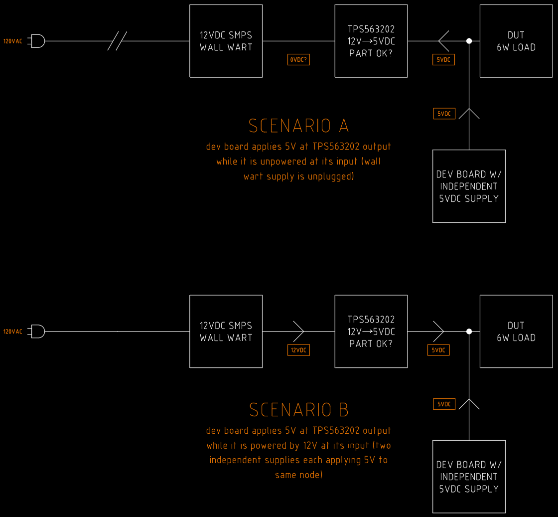
I'm using the TPS563202 in a new design, and it is set to supply 5V on the output.  Normally, the part is powered by a permanently-wired 12V wall wart adapter.  During development efforts, the board the converter is on can also be powered over a flex cable connection that supplies 5V.  The original circuit designers included a TPS22913CYZV switch that is enabled from the converter side in order to isolate it when the board is powered by a dev board and prevent damaging "backfeed" through the converter.  I'm not convinced this switch is necessary, and would very much like to remove it for cost, board area, and thermal savings, and I wondered if TI could offer an opinion.  Here is my reasoning covering the two powered scenarios:

When the external 12V wall wart supply (itself a flyback switcher) isn't plugged in but the board is powered by an external 5VDC source, the low side FET of the TPS563202 will be off and reverse-biased, so no current will flow through that path.  The high side should also be off, but the FET's body diode will be forward biased and will charge the converter's input caps to 5V minus its forward drop, but I can't see how that will damage anything.  If the converter tries to turn on and start switching, the high side switch will charge the input caps such that Vin = Vout but again, I can't see how current would flow in any damaging way.  I guess the worst case is that somehow the low side FET would latch on and offer a short to ground, which would indeed cause damage, but I'd think the internal design of the TPS563202 would prevent that.

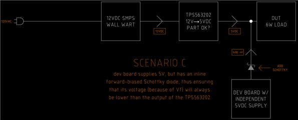
When the external 12V wall wart supply is plugged in and the TPS563202 is outputting 5V, but 5V is also being supplied at the converter's output through the dev board connection, one of the two nominally 5V supplies will be slightly higher than the other one.  If the TPS563202's output is slightly higher than the external supply, then a small amount of current might try to flow in that direction, but it seems like we could easily prevent that by placing a Schottky diode on the dev board so that it would be reverse biased in this case.  If the external dev 5V supply is slightly higher than the TPS563202's set point, I can't see how current will flow back to the input because it is being supplied from 12V.

Is my reasoning sound?  Am I missing something?

Thanks,

Josh

  • Hi Josh!

    Could you please provide a Fig to show the electrical relationship between external source and our TPS563202?

    BSR-MV

    Shuai

  • Thanks for responding Shuai - sure, here it is.  Let me know if this isn't more clear.  Scenario A refers to the second paragraph in my original question, and scenario B refers to the third paragraph.

  • Hi Josh!

    1.For your first concern(wall wart supply plugged out), it is ok. Because 563202 is ECO mode.

    If your target voltage is a little bit higher than DEV board's voltage, the high switch and low switch will be closed.

    If your target voltage is a little bit lower than DEV board's voltage, IC will operate in max duty cycle(0.87 in TPS563202). The input voltage of TPS563202 will be boost to higher than the DEV board voltage. Calculate: 5V/0.87=5.74V. But there won't be large current through in input terminal of  563202.

    Above analysis is just logic level and theoretical. And I am also interested in this, i will test with our EVM board.

    2. For your second part, i have some concern. Are the DEV board and Tps563202 will supply load together? There may exist a problem about current sharing between TPS563020 and DEV board. You can also add a diode in TPS563201's output path.

    Shuai

  • Hi

    Update.

    The first situation has been validated. No problem.

    Shuai

  • Thanks for the responses Shuai - much appreciated.

    Yes, in the second scenario, both 5V supplies would be connected to the same load simultaneously.  I also thought of adding a diode in the TPS563202's output path, but that isn't an acceptable solution because it comes with the significant downsides of the forward voltage drop (with its accompanying efficiency loss and additional heat loading of the system) as well as increased BOM cost and board area.  It wouldn't make sense to increase the cost of every unit sold just to protect against the case of a dev board being connected, which will only happen for a tiny fraction of units produced.  What about putting a Schottky diode in series with the dev board's supply instead?  See scenario C diagram below.

  • Hi

    putting a Schottky diode can achieve what you want. But you should be careful about the current ability of DEV board, because of the current sharing problem.

    Shuai