This thread has been locked.

If you have a related question, please click the "Ask a related question" button in the top right corner. The newly created question will be automatically linked to this question.

TPS65265: TPS65265RHBR, sequence is not as per configuration (power rails are not enabling as per sequence)

Part Number: TPS65265

Hello,

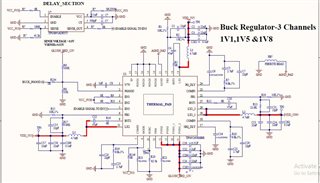
I am working with  "TPS65265RHBR triple channel DC to DC regulator.

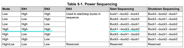
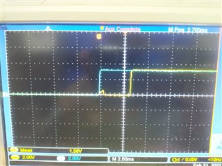
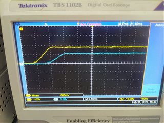
the circuit is configured with a particular power sequence as "BUCK1-<BUCK3->BUCK2".

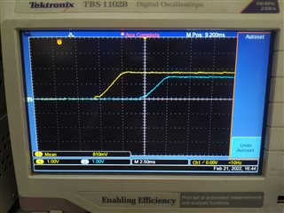
Configured Enables pins as mentioned in the datasheet.

but the sequence is not as per"BUCK1-<BUCK3->BUCK2".

I am getting a power sequence as "BUCK1-<BUCK2->BUCK3".

Between BUcK 1 to BUck 2, I can observe a delay of around (0.2ms -0.3ms), and between Buck 2 to Buck 3,  I can observe a delay of  (2ms to 2.5ms).

So can someone review my schematic and let me know why do I get such an issue.,


NOTE:

Also, I try the below possibility tests too.,

1. I tried connecting the MODE pin to VCC (3.3V) and also by floating the MODE pin but there is no change in a power sequence.
2. Also I tried by connecting PSM pin VCC (3.3v) and also by floating the same pin but there is no change in a power sequence.
3. I tried different delays to EN3 pin as 2ms,10ms,12ms but there is no change in a power sequence.
4. I try to connect the MODE pin to High (TPS65265 IC 1st pin),in the TPS65265 1st pin we get 6V. [This one i tried because in EVK it was mentioned to give to 1st pin of TPS65265 IC for high].but there is no change in a power sequence.
5.

  • Hi

    Our team will reply you next Monday !

    Shuai

  • Hi Karthikeya,

    Thanks for coming to us with your queries.

    1. Could you please connect MODE pin to high(V7V), connect C16(0.01uF) and keep other settings same as your schematic, then probe EN1/EN2/EN3/MODE voltage and probe EN3/BUCK1/BUCK2/BUCK3 output voltage? Please also kindly add some key delay time measurements in the waveform. I want to check the sequence.

    2. Could you please first float MODE pin and keep other settings same as your schematic, then probe EN3/BUCK1/BUCK2/BUCK3 output voltage? Please use different delays to EN3(enable signals to EN3) as 2ms and 10ms and probe both of them. I want to check whether EN3 enable signal and external controlled sequence could function well.

    Thanks!

    BRs

    Lucia

  • Hello Mr.Lucia,

    Thanks for your valuable input.....

    "1. Could you please connect MODE pin to high(V7V), connect C16(0.01uF) and keep other settings same as your schematic, then probe EN1/EN2/EN3/MODE voltage and probe EN3/BUCK1/BUCK2/BUCK3 output voltage? Please also kindly add some key delay time measurements in the waveform. I want to check the sequence."

    I tried by Connecting the MODE pin to V7V (6V, at 1st pin of IC), in this scenario none of the buck regulators are generating its voltage (all the 3 buck channels are giving 0V).

    If I make the MODE pin float or connect it to 3.3V then all 3 channels are generating their output voltages. but if I connect MODE to V7V then none of the channels are generating its output voltage.
    -----------------------------------------------------------------------

    2. Could you please first float MODE pin and keep other settings same as your schematic, then probe EN3/BUCK1/BUCK2/BUCK3 output voltage? Please use different delays to EN3(enable signals to EN3) as 2ms and 10ms and probe both of them. I want to check whether EN3 enable signal and external controlled sequence could function well.

    In this case, I can observe 3 channels are generating output voltage as per configuration. But still no change in a power sequence. (BUck1->Buck2->Buck3) this sequence is only I can see through an oscilloscope.

    -----------------------------------

    I have introduced a 3ms delay for EN3.,
    As per your suggestion, I have introduced a delay between each channel by soldering C16.

    Waveforms are included for your reference.

    1.EN1 to EN3 delay (3ms delay)

    2.EN2 to EN3 dealy (3 ms delay)

    3.BUCK1 (Yellow ) to BUCK2(Blue) there is a 2.5ms delay due to c16.

    .

    --------------------------------------------------------------------------------------

    4.BUCK1(Yellow) to BUCK3(Blue) there is a 5ms delay due to c16.

    .

    ----------------------------------------------------------------------------------------------

    So again i can observe same power sequence of Buck1->Buck2->Buck3.

    but i need Buck1->Buck3->Buck2.

    i hope in between each channel delay is introduced due to C16, but still the power sequence is not working as per datasheet.

  • Hi Karthikeya,

    Thanks for your waveforms and update.

    1. There is one thing which confused me. From your first note, I think this time there still has power sequence even though it is not correct.

    " 4. I try to connect the MODE pin to High (TPS65265 IC 1st pin),in the TPS65265 1st pin we get 6V. [This one i tried because in EVK it was mentioned to give to 1st pin of TPS65265 IC for high].but there is no change in a power sequence."

    However, from your last reply, when the MODE pin is connected to V7V (6V, at 1st pin of IC), in this scenario none of the buck regulators are generating its voltage (all the 3 buck channels are giving 0V). Could you please check which spec or setup has been changed?

    2. When the mode pin is connected to 3v3, could you please help probe EN1/EN2/EN3/MODE voltage in the same figure and also probe EN3/BUCK1/BUCK2/BUCK3 output voltage in the same figure to better check the sequence?

    3. Could you please use a separate external power supply connected to MODE pin and connect MODE to high if it is convenient? I am not sure whether it is because mode pin is not function well.

    4. I will also do some measurements on EVM board following the same setup as yours and give you reply if there is any update. Thanks for understanding. 

    Thanks!

    BRs

    Lucia

  • Hello Lucia,

    Once again thanks for your input.,

    1. Now I can observe the power sequence in the circuit.

    -> Due to my internal board Vcc_3v3 the power sequence was not working properly and also,as like i told if i connect MODE pin to Vcc_3v3 only I can see buck channels generating, its output, (but not in sequence) , if i pull it to v7V none of the bucks are generating its output.(in any sequence).


    -> So individual pull up I gave from the main power supply through voltage dividers as like in EVK kit, to enable pins. (I hope due to some delay in Vcc_3v3 net , the circuit was not functioning properly)


    -> Now the IC can give a proper sequence as per my required configuration.,


    Also few points were noted:-
    1. Only during the Automatic power sequence condition (SEQ-DLY) delay is introduced between each buck.
    2. Only if we pull MODE pin to V7V required sequence is functioning properly, if the MODE pin is left open then none of the sequences is working.
    3. In my power sequence condition even if I left EN1, EN2 as floating or EN1, EN2 to external voltage divider 3v3 voltage, the power sequence is happening as per my configuration.

    Once again thanks for your valuable input...

    Regards

    Karthikeya

  • Hi Karthikeya,

    Thanks for your notes and update. Is the circuit sequence not functioning properly due to Vcc_3V3? What changes do you make to fix this problem for us to better understanding this issue?

    Let me know if you have any more concern.

    Thanks!

    Lucia