This thread has been locked.
If you have a related question, please click the "Ask a related question" button in the top right corner. The newly created question will be automatically linked to this question.
Hello,
Where did you consider the reference (in which pin) in the Referred-to-Input Noise diagram ? (Figure 7 of the datasheet)
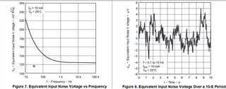
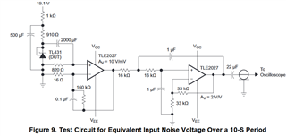
The only test configuration you show for noise tests is the following one. It corresponds to the Figure 8 results.
We would be very interested to have the configuration test or the reference for the noise generator to obtain the RTI noise.
Thank you.
BE,
Hi BE,
You can certainly build the circuit shown to do noise tests. This is because the noise levels on the TL431 are lower than what measurement equipment can see, so it needs to be gained up considerably (in this case, about 20,000x).
When you are saying "referred to input" in this case it means the cathode of the TL431. The reason it is called RTI is because the gain has to be back calculated from output noise to determine input noise (from the voltage reference).
-Tony
Hello,
Thank you for your response.
To be sure to understand your response, can you please put two points in red which indicate each references INPUT and OUTPUT that allow to calculate RTI and RTO on the followings schematics (all cases) :
With you response we would consider that the INPUT for RTI is on the VREF pin (such as in the AOP agreement on the non inverting input pin) and the OUTPUT on the Cathode.
Thank you very much,
Best regards
BE
Hi BE,
See below. Red is input and blue is output. For most of these schematics, they are the same thing.
-Tony