Yes, you can parallel the channels of a dual channel low side driver such as TI’s new UCC27624. This will provide nearly double the drive strength by paralleling the channels. If you as a designer want to avoid the additional work of paralleling two driver channels for extra drive strength, you can also consider TI’s new single channel low side driver, the UCC27614 with 10A source / sink current.
One of the first considerations when paralleling channels is looking at the gate driver “Delay Matching Between Two Channels” specification. Delay matching specifies how well the internal propagation delays between channels are matched. In other words, if the signal is simultaneously applied at the inputs of two channels, the time delay difference at the outputs of both channels is the delay matching specification. The smaller the delay matching specification, the better performing the gate driver is. Using the UCC27624 as an example (see datasheet spec table below), we see the typical delay matching is 1ns and the maximum delay matching is only 2ns! This will give the designer peace-of-mind when connecting the outputs together, as this mitigates the chance of shoot-through both of output stages. Using a gate driver with a maximum delay matching between channels of 2ns is a good rule of thumb.

Caution must be exercised when directly connecting OUTA and OUTB pins together because there is the possibility that any delay between the two channels during turn-on or turn-off may result in shoot-through current conduction as shown in image below.
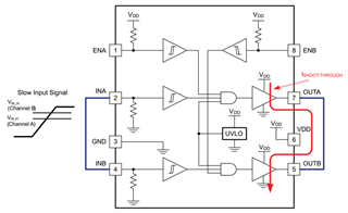
In addition to making sure the delay matching specification is sufficient, it is also important to use an input signal that has a fast rise time of 20 V/µs or greater. This is because there may be small differences in the input threshold voltage level between the two channels, which can cause delay between the two outputs, especially when a slow dV/dt input signal is used.
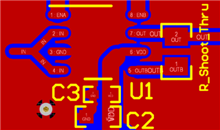
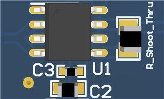
If a designer wants more peace-of-mind or is using a driver with less than desirable delay matching specification, consider placing a resistor in between the two outputs as shown in the schematic below. If shoot-through were to occur, the “R_Shoot_Thru” resistor would help limit the shoot-through current. Designers often put a 0Ω (short) placeholder here to give flexibility later.
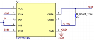
NOTE: Although the UCC27624 has internal pullup resistors for both of the enable pins, and therefore they can be floated; TI recommends that these pins be directly shorted to the VDD pin. If the designer wants to use the enable pins, they must connect the enable pins together as close as possible (just like the input pins).
-------
Layout is another very important part of paralleling driver channels. When creating the PCB layout, design with the following in mind:
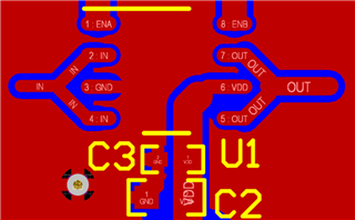
- Inputs must be connected as close as possible to the device (with symmetric traces)
- Outputs must be connected as close as possible to the device (with symmetric traces)
- Optional: Resistor between the two channel outputs can help mitigate risk of shoot-through damage
Please see the two layout examples below as a reference (These examples use the UCC27624D). The first example shows a layout with closely attached traces that are symmetric, on both the input and output pins. The second one shows the same, but with a shoot-through limiting resistor.
