


Hi team,
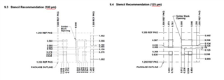
There are two kind of layout spec for out CSD87381. Could you kindly help to confirm the difference between them? Thanks,
Original question:

Hi team,
There are two kind of layout spec for out CSD87381. Could you kindly help to confirm the difference between them? Thanks,
