This thread has been locked.

If you have a related question, please click the "Ask a related question" button in the top right corner. The newly created question will be automatically linked to this question.

TPS65185: Question about 5V cut off (TPS651851RSLR)

Part Number: TPS65185

Hello,

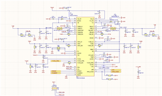
I have a question about PMIC TPS651851RSLR. On our board, 5V supply (for pins 40 (VB_SW) , 24 (VIN_P) and 10 (VIN))

is switched on/off by switching circuit. In this situation, when 5V was cut off, voltage on VIN wasn't cut off, but  changed to about 2V-3V. Maybe it's

because the fact, that after switching PMIC_5V off, there is still 3.3V on pull-up pins (for example I2C or PWR_GOOD), on 45 pin (VIN3P3) and it can be also

on signal lines (for example WAKEUP line). Do you have idea how the voltage is transfered  to VIN pin and if it can be dangerous for PMIC in

that state (5V cut off and 3.3V on pull-up lines, on VIN3P3 pin and on signal lines) ?

  • I'm adding the part of schematic

  • Hi Bartosz,

    It is possible there is a leakage path between one of these pins and the 5V supply input pins. It would be recommended to avoid this state (leakage voltage present on 5V input) if possible. By removing 3.3V on any of the pulled-up pins, are you able to narrow down to a pin that is responsible? This would determine if an internal leakage path is the root cause. If so, we can look further into the design to determine what is creating the leakage. 

    Just one comment on your schematic:

    • VPOS_IN and VB can share C54 this these pins are adjacent. Dedicate C62 to VDDH_IN.

    Thanks,

    Gerard

  • Hello Gerard,

    Thank you for the answer and comment about schematic.
    Some "narrowing down" has already been done. After
    removing pull-up form SDA, SCL, PWR_GOOD and INT lines
    and cutting the trace (to break connection) close to 45 pin (VIN3P3),
    the voltage VPMIC was about 2.4V. Before those operations it was about 3V,
    so there was some voltage change, but not to 0V, so maybe more than one pin,
    is responsible for this situation, also signal pins like PWRUP, WAKEUP or VCOM_CTRL. 

  • Hi Bartosz,

    Understood that removing 3V3 from SDA, SCL, PWR_GOOD, and INT reduced the voltage at VIN to 2.4 V. What was the effect of removing 3V3 from PWRUP, WAKEUP, and VCOM_CTRL?

    Thanks,

    Gerard

  • Hello Gerard,

    It turned out, that WAKEUP, PWRUP and  VCOM_CTRL were in 0V state, but it turned out also,
    that voltage from I2C lines wasn't disconnected despite the fact of removing pull up resistors.
    Maybe it's because of internal structure of other unit connected to I2C bus. Connecting SDA and SCL lines to GND
    (via resistors 100R) caused input VPMIC voltage change to about 0.002V, so almost to 0V. Earlier some VPMIC voltage drop (from about 3V to about 2.4V)  was observed after removing R37 and R38 pull up resistors, so maybe few signal lines influence the voltage, which appears on the input even if supply is not connected. To sum up, there is some voltage transfer to 40, 24 and 10 pins in situation when 5V is disconnected and 3.3V is connected to some pins of  the PMIC. Do you know if it can be dangerous for TPS651851RSLR in longer time in this state?

  • Hi Bartozs, 

    Thanks for the update on your testing. The best approach is to understand why 3.3 V remains present on the I2C bus and whether it is preventable. It is not recommended to enable internal leakage paths through the PMIC pins. Has this behavior been observed on multiple devices?

    Additionally, there is risk to the system components if the PMIC powers up unexpectedly due to the residual voltage. The PMIC's input UVLO is 2.9 V, which is within the range of the measured voltage (you mentioned 2-3 V). If WAKEUP/PWRUP/VCOM_CTRL are asserted in this scenario, the PMIC will power up, potentially damaging the downstream components if the power up is not expected. 

    Thanks,

    Gerard

  • Hello Gerard,

    Voltage about 3V was observed on PMIC VIN in different boards, so problem probably is not caused by defect of one piece.
    Thank you very much for your help and explanation. Maybe we will change our design to constant 5V input with switching
    to sleep mode using WAKEUP line.I think, we can close this topic now. Thank you.

  • Hi Bartosz, 

    This sounds like a good alternative to prevent the issue as long as the PMIC's quiescent power consumption has been determined acceptable by the customer. Please feel free to start a new thread if any more questions come up. 

    Thanks,

    Gerard