This thread has been locked.

If you have a related question, please click the "Ask a related question" button in the top right corner. The newly created question will be automatically linked to this question.

LM5143-Q1EVM-2100: Start-up process

Part Number: LM5143-Q1EVM-2100
Other Parts Discussed in Thread: LM5143

Hi team,

In our LM5143EVM,there is a start-up characteristic showing as following:

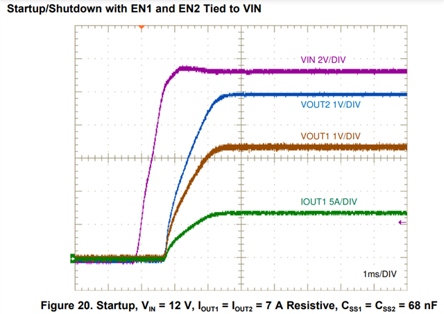
With the Css=68nF setup, the calculated soft start time should be 1.94ms, but I am little confusing about the 1.9ms time division.

In above waveform, there is a no swtiching stage after Vin is over UVLO threshold which is 0.9ms roughly; and then the output voltage rising stage is 1ms;

So what is the first stage for?  And the calculated SS time is usual the stage 1 + Stage 2 Vo rising, if this understanding is right?

Thanks.

Best regards

Mia Ma

  • Hi Mia,

    There is some delay to charge the VCC capacitor and subsequently release the SS voltage. Then the COMP voltage must increase to initiate switching. The SS time is calculated based on the SS voltage going from 0V to 0.8V.

    Regards,

    Tim

  • Hi Timothy,

    Thanks for your quick response and clear about the soft start question.

    And I have some more application question want to confirm with you:

    Q1:Will our LM5143 thermal status changed by output power level or output voltage?

    Q2:From my understanding,LM5143 consumped power loss will not change anymore after the Vin,fsw and FET type fixed in a design. But my customer recently find out if they lower the output(5V to 3.3V), the LM5143 temp will have a obvious increasement,if this is normal?

    Q3:Any method we could optimize the LM5143 thermal performance based a fixed parameter design?

    Thanks a lot.

    Best regards

    Mia Ma

  • Hi MIa,

    The LM5143 power dissipation is mainly related to the VCC current related to FET gate switching. The VCC current applicable to each FET is Icc = Fsw*Qg.

    The VCC current is normally derived from VIN, unless VCCX is powered (>=4.3V). If the output was changed from 5V to 3.3V, then the external bias was not possible and hence the IC power dissipation increased.

    Regards,

    Tim